🇺🇸 Chips of the United States
733 chips from the United States, best known first.
The United States has launched a major federal programme to rebuild its domestic semiconductor supply chain. New legislation directs tens of billions of dollars toward building fabrication plants, funding research centres, and training engineers. These measures aim to reduce reliance on foreign suppliers while restricting advanced chip production in rival nations.
- Legislation allocates $52.7 billion in direct appropriations for chip manufacturing.
- Subsidy recipients cannot produce transistors smaller than 28 nanometres in China or Russia.
- Tax credits cover 25% of approved fabrication equipment purchases.
- Programmes aim to create between 25,000 and 45,000 new technical jobs.
- Empty factory construction allows firms to secure funding before installing heavy machinery.
Chips in the United States
American semiconductor manufacturing relies on a mix of domestic design houses and international partners. To secure this supply chain, the federal government introduced a sweeping industrial policy focused on local production. The strategy centres on financial incentives for constructing new fabrication facilities, known as foundries, where raw silicon wafers are etched into complex circuit patterns. It also channels money into academic research and technical education. By tying public funds to national security goals, the programme seeks to keep critical hardware development within American borders. This approach reshapes how the nation approaches microelectronics, moving from passive market dependence to active state sponsorship.
History
The legislative framework emerged from two separate proposals merged in early 2022. Lawmakers combined a technology research bill with a manufacturing incentive plan to address growing supply vulnerabilities. Key senators drafted the initial versions after diplomatic efforts encouraged overseas producers to consider American sites. The final package cleared both chambers with cross party backing before receiving presidential approval. Earlier drafts had proposed larger funding pools and broader regional innovation networks, but the enacted version narrowed its scope to focus primarily on microelectronics and allied scientific fields.
Companies
Major manufacturers have adjusted their expansion plans to align with the new funding rules. Some firms are constructing empty factory shells before purchasing heavy machinery, a tactic designed to avoid future market oversupply. International producers previously discussed relocating assembly lines to American soil to access these incentives. Domestic leaders have welcomed the financial support while expressing caution about the restrictions placed on overseas operations. Industry representatives generally back the initiative, though they worry that compliance requirements might slow down rapid facility upgrades.
Fabs and places
New fabrication plants, or foundries, will concentrate on producing logic chips and memory devices. The legislation encourages construction across multiple states, with several existing industrial zones selected for redevelopment. Recipients must commit to maintaining these facilities for a decade and cannot expand advanced node production in certain Asian markets. Advanced nodes refer to transistor sizes smaller than 28 nanometres, which require precise lithography equipment. The rules also mandate that funded sites hire local workers and partner with technical colleges to build a steady talent pipeline.
Policy and support
Federal agencies distribute grants and loan guarantees through a structured application process. Companies receive tax credits covering 25% of their equipment costs, alongside direct cash awards for facility construction. A portion of the budget supports university programmes, public research institutes, and workforce development initiatives. The law also establishes ethics guidelines and security protocols for all funded laboratories. Recipients face strict export controls, including a 10-year prohibition on developing cutting edge processors for restricted countries. Bureaucratic processing times remain lengthy, and some research allocations have faced congressional reductions.
Today
Recent assessments indicate that the programme has triggered dozens of proposed manufacturing and research ventures. Analysts project hundreds of billions in private capital will follow the initial public commitments. Employment forecasts suggest 25,000–45,000 new technical roles will emerge across engineering and plant operations. Implementation continues to navigate administrative bottlenecks and labour market gaps. Despite these friction points, the funding architecture remains active, guiding capital toward domestic semiconductor infrastructure and sustaining long term investment cycles in the national electronics sector.
The facts in this overview come from the Wikipedia article "CHIPS and Science Act", written by its contributors and used under the CC BY-SA 4.0 licence. EveryChip rewrote the text in its own words, with AI assistance, and compares every page with the article to make sure no passage is copied. It may be reused under the same CC BY-SA 4.0 licence with a link back.
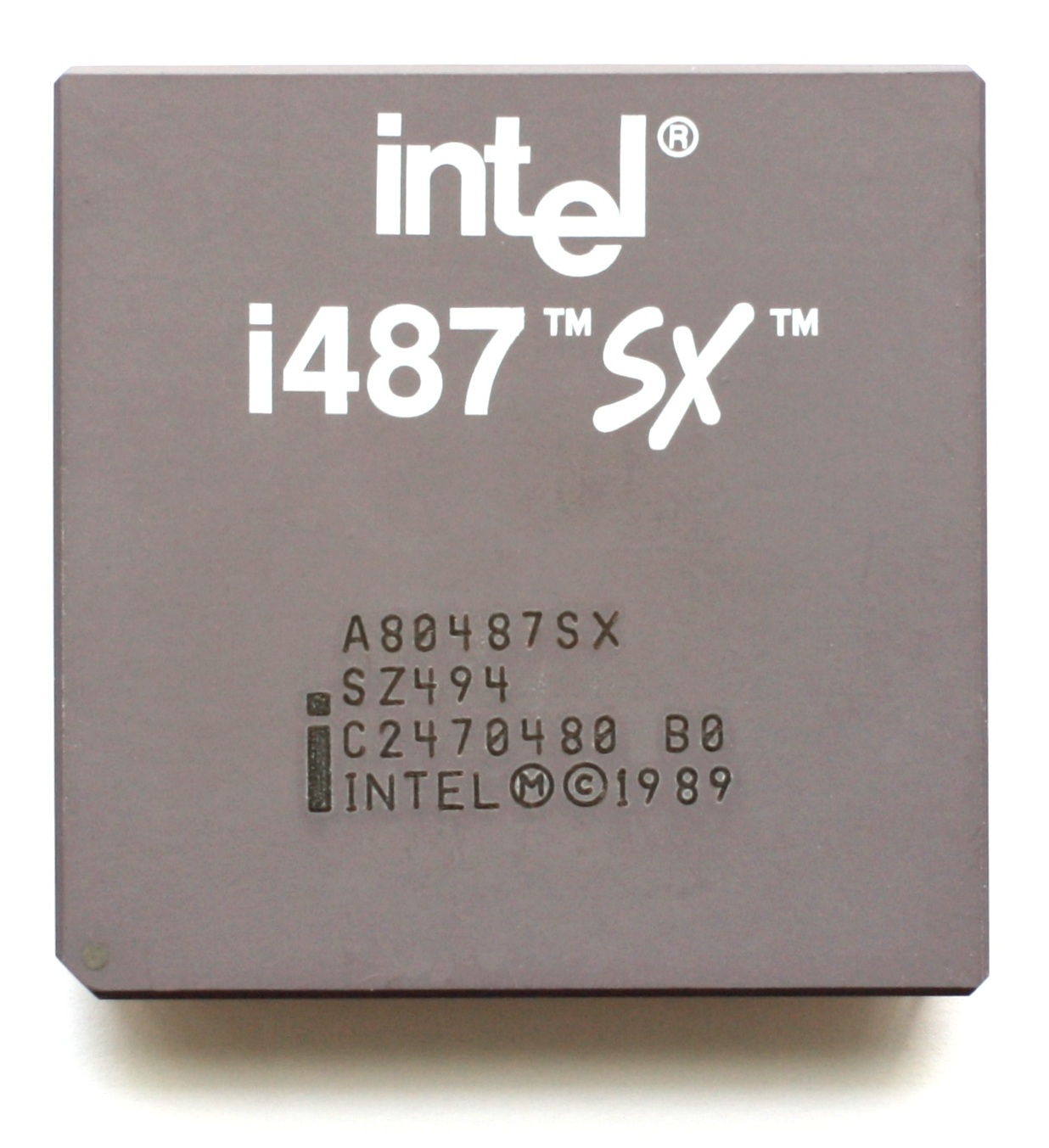 🇺🇸 United StatesIntel 80487SX
Floating-point upgrade chip for Intel 486SX systemsCPU · x86 · 1991
 🇺🇸 United StatesV-11
DEC's first complete VAX microprocessor chip setCPU · Other · 1986
🇺🇸 United StatesMicroBlaze
Soft microprocessor core for Xilinx FPGAsFPGA · RISC · 2002
 🇺🇸 United StatesMasPar MP-2 PE
32-element SIMD processor chip for MasPar supercomputersCPU · Other · 1987
 🇺🇸 United StatesPC100
Intel standard for reliable 100 MHz SDRAM modulesMemory
🇺🇸 United StatesLatticeMico8
8-bit RISC soft processor core for FPGAsMicrocontroller · RISC
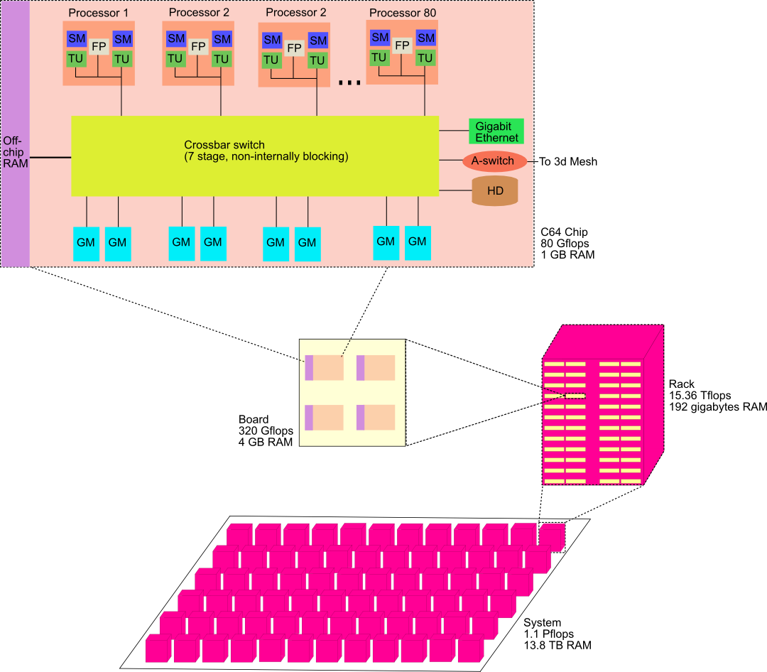 🇺🇸 United StatesCyclops64
IBM cellular architecture aiming for a supercomputer on a single chip.CPU · Power
🇺🇸 United StatesHandy Board
Open-source handheld robotics controller based on 68HC11 microcontrollerMicrocontroller · 68k
🇺🇸 United StatesAMD FireStream
GPGPU co-processor cards for supercomputing and stream processing.GPU · GPU architecture · 2006
🇺🇸 United StatesExtreme Graphics
High-end graphics architecture for SGI workstationsGPU · Other · 1993
🇺🇸 United StatesIMPACT
High-end graphics architecture for SGI workstationsGPU · Other · 1995
 🇺🇸 United StatesRealityEngine
High-end 3D graphics hardware by Silicon GraphicsGPU · Other · 1992
 🇺🇸 United StatesInfiniteReality
High-end 3D graphics architecture by Silicon GraphicsGPU · MIPS · 1996
 🇺🇸 United StatesSBP0400
4-bit slice microprocessor using I²L technologyCPU · Other · 1975
🇺🇸 United StatesIntel 8283
8-bit latch for Intel 8086 processor systemsAnalog
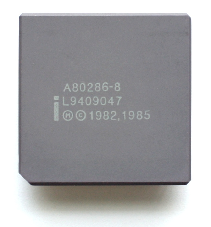 🇺🇸 United StatesIntel 80286
16-bit microprocessor with protected mode and 16 MB memory supportCPU · x86 · 1982
 🇺🇸 United StatesCharge-coupled device
Integrated circuit sensor that converts light into digital images.Sensor · 1969
 🇺🇸 United StatesTRIPS
Experimental EDGE processor from University of Texas at AustinCPU · Other
🇺🇸 United StatesField-programmable object array
Programmable logic device bridging FPGA and ASIC gapsFPGA · Other · 2006
 🇺🇸 United StatesQuantum well infrared photodetector
Infrared sensor using quantum wells for detectionSensor · 1987
 🇺🇸 United StatesGeForce 800M series
Nvidia laptop graphics chips from 2014 using Fermi, Kepler and Maxwell designs.GPU · GPU architecture · 2014
 🇺🇸 United StatesBubble memory
Non-volatile magnetic storage using moving domains in thin filmsMemory · 1967
 🇺🇸 United StatesIntel 430HX
Socket 7 chipset for Pentium and MMX processorsAnalog · 1996
 🇺🇸 United StatesApple W2
Wireless connectivity chip for Apple Watch Series 3SoC · Arm
 🇺🇸 United StatesTI-AR7
Single-chip ADSL router solution with MIPS processor and DSPSoC · MIPS
 🇺🇸 United StatesApple S6
System in a package for the Apple Watch Series 6SoC · Arm · 2020
🇺🇸 United StatesIntegrated Facility for Linux
IBM processor dedicated to running Linux workloadsCPU · Other · 2000
🇺🇸 United StatesPhysX P1
Dedicated microprocessor for video game physics calculationsCPU · MIPS · 2006
 🇺🇸 United StatesHopper
Nvidia datacentre GPU microarchitecture for AI and high-performance computing.GPU · GPU architecture · 2022
 🇺🇸 United StatesMicrobolometer
Uncooled infrared sensor for thermal imaging camerasSensor · 1992
 🇺🇸 United StatesAI Engine
AMD hardware architecture for AI inference and signal processingAI accelerator · VLIW
 🇺🇸 United StatesIBM 2361
Magnetic core memory expansion for IBM System/360 mainframesMemory
 🇺🇸 United StatesAVR Butterfly
Wearable single-board microcontroller demo kitMicrocontroller
🇺🇸 United StatesPower Processing Element
64-bit PowerPC core for PlayStation 3 and Xbox 360CPU · Power · 2005
 🇺🇸 United StatesOPD Mini Processor
Proprietary 16-bit microprocessor for IBM word processorsCPU · Other · 1977
🇺🇸 United StatesProgrammable metallization cell
Non-volatile resistive memory using metal filamentsMemory
 🇺🇸 United StatesTigerton
Intel Xeon processor model released in 2005 for servers.CPU · x86 · 2005
 🇺🇸 United StatesULLtraDIMM
Flash storage module for DDR3 memory slotsMemory
 🇺🇸 United StatesCommodore REU
External RAM expansion modules for Commodore home computersMemory · 1986
 🇺🇸 United StatesApple H2
System on a chip for Apple audio and tracking devicesSoC · Arm
 🇺🇸 United States3Com 3c509
ISA Ethernet network card series by 3ComNetwork chip · 1992
🇺🇸 United StatesIBM 2395 Processor Storage
Main memory unit for IBM System/360 mainframesMemory
🇺🇸 United StatesApple U1
Ultra-wideband system on a chip for spatial awarenessSoC · Arm · 2019
🇺🇸 United StatesXDNA
AMD microarchitecture for neural processing units in Ryzen AI chipsAI accelerator · VLIW · 2023
 🇺🇸 United StatesZilog Z8000
A 16-bit microprocessor architecture from Zilog launched in 1979.CPU · Other · 1979
 🇺🇸 United StatesApple S1
System in package for the first Apple WatchSoC · Arm · 2015
🇺🇸 United StatesIntel 80130
Support chip for 8086 processors and iRMX86 OSMicrocontroller · x86
 🇺🇸 United StatesPentium
Intel's first superscalar x86 microprocessor, introducing dual pipelines and the Pentium brand in 1993.CPU · x86 · 1993
Photo credits on this page
The small pictures above come from Wikimedia Commons under free licences. Some are cropped to fit.
- Intel 80286: Konstantin Lanzet (with permission), CC BY-SA 3.0, source
- Granite Rapids: Intel Corporation, Public domain, source
- Intel 80487SX: Konstantin Lanzet (with permission), CC BY-SA 3.0, source
- V-11: Adamantios, CC BY-SA 3.0, source
- PC133: Vitaly Zdanevich, CC0, source
- MasPar MP-2 PE: SmashIt, CC BY-SA 4.0, source
- Cyclops64: Unknown author, CC BY-SA 3.0, source
- RealityEngine: Retro-Computing Society of Rhode Island, CC BY-SA 3.0, source
- InfiniteReality: htomari, CC BY-SA 2.0, source
- SBP0400: Kungfuman, CC BY 3.0, source
- Charge-coupled device: Merzperson ( talk ) ( Uploads ), Public domain, source
- Apple S1: Henriok, CC0, source
- Zilog Z8000: Tiziano Garuti ( 1000Bit, Public domain, source
- Quantum well infrared photodetector: SK, CC BY-SA 4.0, source
- Apple U1: Henriok, CC0, source
- Pentium: Pdesousa359, CC BY-SA 3.0, source
- TRIPS: Toren Smith, CC BY-SA 3.0, source
- GeForce 800M series: PantheraLeo1359531, CC BY 4.0, source
- Bubble memory: DMGualtieri, CC BY-SA 3.0, source
- Intel 430HX: Rjluna2, CC BY-SA 4.0, source
- Apple W2: Henriok, CC0, source
- TI-AR7: Raimond Spekking, CC BY-SA 4.0, source
- Apple S6: Henriok, CC0, source
- Hopper: 极客湾Geekerwan, CC BY 3.0, source
- Microbolometer: Unknown author, Public domain, source
- AI Engine: Dmitry Grigoriev, CC BY 2.0, source
- IBM 2361: Bubba73 , Jud McCranie, CC BY-SA 4.0, source
- AVR Butterfly: Mrbill, CC BY-SA 2.5, source
- OPD Mini Processor: Norsk Teknisk Museum, CC BY-SA 3.0, source
- ULLtraDIMM: FlashStorage, CC BY-SA 3.0, source
- Commodore REU: Unknown author, Public domain, source
- 3Com 3c509: Dmitry Nosachev, CC BY-SA 4.0, source