Power Processing Element
64-bit PowerPC core for PlayStation 3 and Xbox 360
The Power Processing Element is a 64-bit microprocessor core designed by IBM. It launched in 2005 to power the PlayStation 3 and Xbox 360 consoles. The chip also served in supercomputers like the IBM Roadrunner.
- Clock speeds range from 2.8 GHz to 3.2 GHz
- Features a 23-stage pipeline with delay paths
- Used in PlayStation 3 and Xbox 360 consoles
- Supports dual hardware threads on one core
- Manufactured at 90 nm, 65 nm, and 45 nm nodes
What it is
The Power Processing Element acts as the main central processing unit in several notable systems. IBM designed this 64-bit core to handle general computing tasks while other units managed specialized workloads. It supports the PowerPC 2.02 instruction set and includes AltiVec vector processing capabilities. The element combines a Power Processing Unit with a substantial level two cache. This design allowed it to serve as the brain for major gaming consoles and high performance scientific machines.
How it came about
Development involved collaboration between IBM, Sony, and Toshiba. The goal was to create a versatile core for the Cell Broadband Engine architecture. Production began in 2005 with initial manufacturing at 90 nanometres. Later revisions shrank the process to 65 and 45 nanometres. Microsoft also adopted a variant for the Xbox 360, known as XCPU. This cross-industry adoption highlighted its flexibility beyond just Sony products.
Inside the chip
The core features a 23-stage pipeline with extra stages for microcode and branch prediction. It executes instructions in order but can bypass cache misses to maintain flow. Up to eight load instructions may queue out of order during these delays. Dual hardware threads run simultaneously on shared execution resources. Registers for exceptions and interrupts are duplicated for each thread. The floating point unit performs twelve operations per cycle using multiply-add logic.
How it was made
IBM manufactured the chips using processes ranging from 90 to 45 nanometres. The standard Cell version appeared in three size reductions over time. The PowerXCell 8i variant used only the 65 nanometre process. This specific version improved floating point performance for scientific calculations. The physical packaging details remain unstated in the provided documentation.
Where it went
Sony integrated the element into the PlayStation 3 console. Microsoft used a three-core configuration in the Xbox 360. The Xbox version included a unified one megabyte level two cache. Some later Xbox chips combined graphics processing from ATI. Supercomputers like the IBM Roadrunner utilized the core for high performance tasks. The PowerXCell 8i variant targeted scientific computing with enhanced memory subsystems.
Versions and family
Three main implementations exist. The Cell Broadband Engine powers the PlayStation 3. The PowerXCell 8i offers better floating point precision for servers. The XCPU serves the Xbox 360 with modified vector registers. The Xbox graphics integration created the XCGPU variant. IBM eventually succeeded this architecture with the A2 core. Each variant adjusted cache sizes or manufacturing nodes to fit its host device.
Why it matters
This core helped define the seventh generation of video game consoles. Its use in the IBM Roadrunner demonstrated viability in supercomputing. The design proved that in-order execution could achieve high throughput with smart caching. It bridged consumer electronics and scientific research hardware. The collaboration model set a precedent for future custom silicon projects.
Questions people ask about Power Processing Element
What is the difference between PPE and PPU?
The Power Processing Element includes the Power Processing Unit core plus a 512 KB level two cache. The PPU is just the processor core itself. Most systems use the full PPE package for better performance.
Which consoles used this processor?
Sony used it in the PlayStation 3 as part of the Cell Broadband Engine. Microsoft used a modified three-core version called XCPU in the Xbox 360. Both consoles relied on this IBM-designed architecture.
Is the processor out-of-order or in-order?
It is an in-order processor. However, it can execute past cache misses and send load instructions out of order. This hybrid approach avoids stalls without complex reordering hardware.
Good reading and sources
The facts on this page come from the Wikipedia article "Power Processing Element", written by its contributors and used under the CC BY-SA 4.0 licence, and from its Wikidata record (CC0). EveryChip rewrote the text in its own words, with AI assistance, and compares every page with the article to make sure no passage is copied. It may be reused under the same CC BY-SA 4.0 licence with a link back.
It may contain mistakes, and figures change over time. Nothing here is investment or buying advice. If something is wrong, tell us. Last refreshed 2026-11-14.
Like Power Processing Element
All CPUs and microprocessors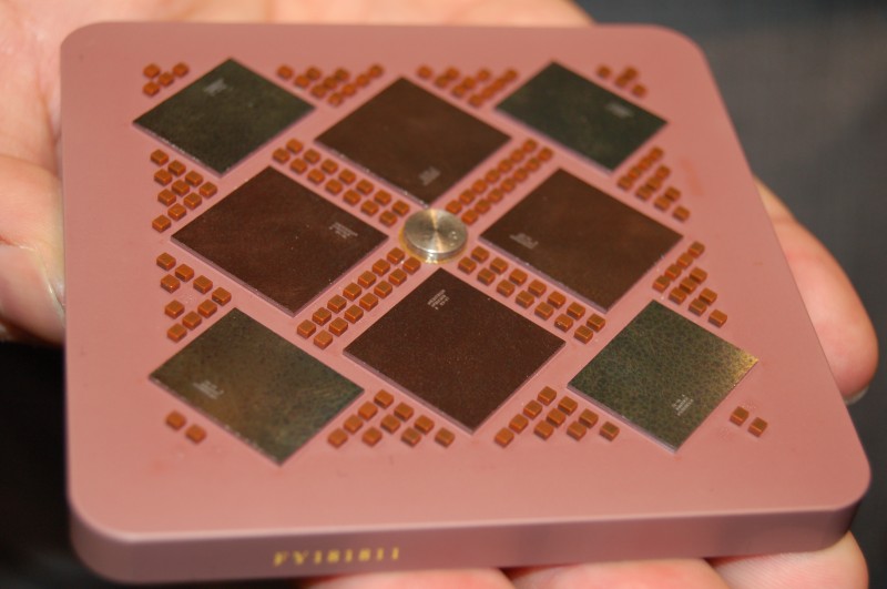 🇺🇸 United StatesPOWER5
Dual-core server microprocessor with simultaneous multithreadingCPU · Power · 2004
 🇺🇸 United StatesBroadway
32-bit PowerPC CPU for the Nintendo Wii consoleCPU · Power · 2006
 🇺🇸 United States and 1 moreMicrosoft XCPU (Xenon)
Three-core PowerPC CPU at the heart of the Xbox 360 consoleCPU · Power · 2003
 🇺🇸 United StatesCell Broadband Engine
A multi-core RISC processor pairing one PowerPC core with eight vector coprocessors.CPU · Power · 2007
More from IBM
All of them 🇯🇵 JapanSpursEngine
Toshiba media coprocessor for video and 3D tasksCPU · Other · 2007
 WorldPOWER6
Dual-core IBM server microprocessor with hardware decimal mathCPU · Power · 2007
🇺🇸 United StatesMillipede memory
IBM experimental non-volatile memory using atomic force probesMemory · 2003