POWER5
Dual-core server microprocessor with simultaneous multithreading
The POWER5 is a dual-core microprocessor designed and made by IBM. Released in 2004, it introduced simultaneous multithreading and an on-die memory controller to enterprise servers. It succeeded the POWER4 and was later refined as the POWER5+ using a smaller manufacturing process.
- First IBM POWER chip with simultaneous multithreading support
- Integrates memory controller directly on the processor die
- Fabricated using 130 nm silicon on insulator technology
- Supports up to 64 GB of DDR and DDR2 memory per chip
What it is
The POWER5 is a microprocessor created by IBM for high-end computing systems. It launched in 2004 as an enhancement to the earlier POWER4 design. This chip features two physical cores that can handle four logical threads at once through simultaneous multithreading. It also integrates a memory controller directly onto the silicon die. These changes aimed to boost performance in enterprise server environments where multiple tasks run concurrently.
How it came about
IBM first shared technical details at the Hot Chips conference in 2003. A fuller description followed at the Microprocessor Forum in October of that year. The chip entered the market in 2004, targeting the enterprise server sector. It competed against processors like the Intel Itanium 2 and Sun Microsystems UltraSPARC IV. In October 2005, IBM released an improved version called POWER5+, which used a more advanced manufacturing process to reduce power usage and size.
Inside the chip
This processor uses the PowerPC 2.02 instruction set architecture. Each of its two cores supports one physical thread and two logical threads. To enable this, IBM duplicated components like the return stack and instruction buffer for each thread. Shared resources, such as register files, were expanded to maintain performance. The chip includes 120 integer and floating-point registers each. An on-die controller manages up to 64 GB of DDR or DDR2 memory. The L2 cache holds 1.875 MB, while a shared 36 MB L3 cache sits on the package.
How it was made
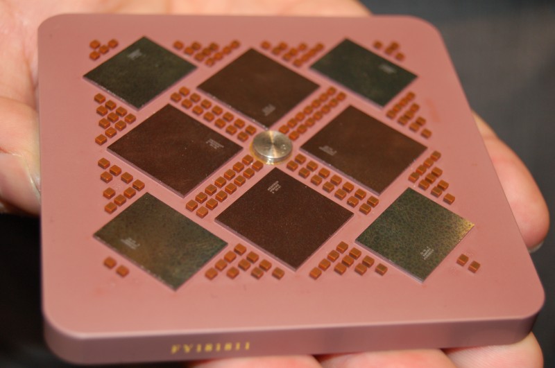
IBM fabricated the original POWER5 using a 130 nm silicon on insulator process with copper interconnects. The die contains 276 million transistors and covers 389 square millimetres. It ships in dual chip modules or multi-chip modules. The latter packs four processor dies and four cache dies into a 95 mm square package. The later POWER5+ moved to a 90 nm process, shrinking the die to 243 square millimetres and allowing higher clock speeds up to 2.3 GHz.
Where it went
IBM integrated these chips into its System p and System i server lines. They also powered DS8000 storage servers and high-end Infoprint printers. Workstations like the IntelliStation POWER 285 used the dual chip module variant. External partners included Groupe Bull for Escala servers and Hitachi for SR11000 computers. Some Hitachi systems with up to 128 POWER5+ processors appeared on the 2007 TOP500 supercomputer list.
Versions and family
The main successor to the POWER4 was the POWER5. An iterative update, the POWER5+, arrived in late 2005. This variant reduced power consumption and die size by moving to a 90 nm fabrication node. While initial clock speeds remained similar, later updates pushed frequencies to 2.3 GHz. The POWER5+ also introduced a quad-chip module package containing two processor dies and two cache dies. The entire line was eventually replaced by the POWER6.
Why it matters
The POWER5 brought simultaneous multithreading to IBM’s high-end server lineup. This allowed better utilisation of execution units when one thread waited for data. By integrating the memory controller, it reduced latency for data access. The technology supported Virtual Vector Architecture, linking multiple processors to act as a single vector unit. Its presence in top supercomputers demonstrated its capability in heavy computational workloads during the mid-2000s.


Questions people ask about POWER5
What is simultaneous multithreading in the POWER5?
Simultaneous multithreading allows the processor to execute instructions from two different threads at the same time on each core. This helps keep the execution units busy when one thread is waiting for data, improving overall efficiency.
How much cache memory does the POWER5 have?
Each core has 32 KB of L1 instruction and 32 KB of L1 data cache. The chip shares a 1.875 MB L2 cache. Additionally, there is a 36 MB L3 cache located on the package, shared by both cores.
What is the difference between POWER5 and POWER5+?
The POWER5+ uses a smaller 90 nm manufacturing process compared to the 130 nm process of the original. This reduces the die size and power consumption. Later versions of the POWER5+ also achieved higher clock speeds up to 2.3 GHz.
Good reading and sources
The facts on this page come from the Wikipedia article "POWER5", written by its contributors and used under the CC BY-SA 4.0 licence, and from its Wikidata record (CC0). EveryChip rewrote the text in its own words, with AI assistance, and compares every page with the article to make sure no passage is copied. It may be reused under the same CC BY-SA 4.0 licence with a link back.
It may contain mistakes, and figures change over time. Nothing here is investment or buying advice. If something is wrong, tell us. Last refreshed 2026-11-14.
Like POWER5
All CPUs and microprocessors WorldPOWER6
Dual-core IBM server microprocessor with hardware decimal mathCPU · Power · 2007
🇺🇸 United StatesIBM A2
Open source 64-bit Power ISA processor core for embedded systemsCPU · Power · 2010
 🇺🇸 United StatesPOWER3
64-bit PowerPC microprocessor for IBM workstations and serversCPU · Power · 1998
 🇺🇸 United States and 1 morePOWER7
IBM multi-core server processor from 2010CPU · Power · 2010
More from IBM
All of them 🇺🇸 United States and 1 moreMicrosoft XCPU (Xenon)
Three-core PowerPC CPU at the heart of the Xbox 360 consoleCPU · Power · 2003
🇺🇸 United StatesPower Processing Element
64-bit PowerPC core for PlayStation 3 and Xbox 360CPU · Power · 2005
🇺🇸 United StatesMillipede memory
IBM experimental non-volatile memory using atomic force probesMemory · 2003
 🇺🇸 United StatesPowerPC 970
IBM's 64-bit PowerPC desktop CPU family, sold by Apple as the G5.CPU · Power · 2002