
POWER6
Dual-core IBM server microprocessor with hardware decimal math
The POWER6 is a dual-core microprocessor designed by IBM and released in 2007. It implements the Power ISA v.2.05 and features hardware support for decimal floating-point arithmetic. Built on a 65 nm process, it succeeded the POWER5+ as IBM's flagship server chip.
- First processor with hardware decimal floating-point unit
- Operates at frequencies up to 5.0 GHz
- Contains 790 million transistors on 65 nm process
- Supports up to 448 cores in water-cooled frames
What it is
The POWER6 is a microprocessor developed by IBM for high-performance servers and supercomputers. Released in June 2007, it implements version 2.05 of the Power Instruction Set Architecture. This chip serves as the successor to the POWER5+ and acts as the flagship processor for IBM’s server line during its production window. It is notable for integrating hardware support for decimal arithmetic, a feature critical for financial and commercial applications that require precise numerical calculations without rounding errors common in binary systems.
How it came about
IBM first described the processor at the International Solid-State Circuits Conference in February 2006. Further technical details emerged later that year at the Microprocessor Forum. The company formally announced the chip on May 21, 2007, with general availability following on June 8. Initial models operated at speeds between 3.5 and 4.7 GHz. By May 2008, IBM introduced the P595 system, which bumped the maximum frequency to 5.0 GHz. The design effort was part of the eCLipz project, aiming to converge hardware across IBM’s iSeries, pSeries, and zSeries product lines.
Inside the chip
This dual-core chip contains approximately 790 million transistors. Each core supports two-way simultaneous multithreading. Unlike its predecessor, the POWER6 executes instructions in order rather than out of order. This architectural shift often requires software recompilation for optimal speed, though performance gains remain significant even with unmodified code. Each core includes two integer units, two binary floating-point units, an AltiVec unit, and a dedicated decimal floating-point unit. The latter handles IEEE 754 decimal arithmetic directly in silicon. Cache memory includes 64 KB instruction and data caches per core, a semi-private 4 MB unified L2 cache, and a shared 32 MB off-die L3 cache.
How it was made
The processor is fabricated using a 65 nm process technology. IBM addressed power leakage issues associated with high frequencies by combining 90 nm and 65 nm components within the design. The chip uses a copper distribution wire for its clock network, measuring 3 micrometres wide and 1.2 micrometres thick. It operates with dual power supplies: a logic supply ranging from 0.8 to 1.2 Volts and an SRAM supply roughly 150 millivolts higher. The physical die size is 341 square millimetres. Thermal characteristics remain similar to the previous POWER5 generation.
Where it went
Systems based on this processor include Express models like the 520, 550, and 560, targeting small businesses. Enterprise models such as the 570 and 595 serve large data centres with features like hot-pluggable memory books. IBM also offered four blade server variants supporting AIX, IBM i, and Linux operating systems. For high-performance computing, the water-cooled Power 575 system uses nodes with 32 cores each. These clusters can scale up to 448 cores in a single frame, making them suitable for scientific simulations and heavy computational workloads.
Versions and family
An enhanced version called POWER6+ began shipping in October 2008 within Power 560 and 570 systems before its formal introduction in April 2009. This variant added more memory keys for secure memory partitioning, a technology borrowed from IBM mainframes. The original POWER6 was succeeded by the POWER7 processor. The z10 mainframe microprocessor also shares significant technology with the POWER6, particularly regarding decimal floating-point support.
Why it matters
The inclusion of a hardware decimal floating-point unit marked a significant step for commercial computing accuracy. This feature allowed financial applications to perform precise calculations without software emulation overhead. The processor supported up to 31 other processors via high-speed inter-node links. It also enabled up to 10 logical partitions per core, facilitating efficient resource allocation in virtualised server environments. The design influenced subsequent IBM chips, including the z10 mainframe processor.


Questions people ask about POWER6
What makes the POWER6 different from previous IBM processors?
The POWER6 executes instructions in order instead of out of order. It also includes the first hardware decimal floating-point unit integrated in silicon, allowing precise decimal arithmetic for financial applications without software emulation.
How many cores does the POWER6 have?
The POWER6 is a dual-core processor. Each core supports two-way simultaneous multithreading, allowing it to handle four threads concurrently. The cores share a 32 MB off-chip L3 cache.
What manufacturing process was used for the POWER6?
IBM fabricated the POWER6 using a 65 nm process. The design combines 90 nm and 65 nm parts to manage power leakage at high frequencies. The die size is 341 square millimetres.
Good reading and sources
The facts on this page come from the Wikipedia article "POWER6", written by its contributors and used under the CC BY-SA 4.0 licence, and from its Wikidata record (CC0). EveryChip rewrote the text in its own words, with AI assistance, and compares every page with the article to make sure no passage is copied. It may be reused under the same CC BY-SA 4.0 licence with a link back.
It may contain mistakes, and figures change over time. Nothing here is investment or buying advice. If something is wrong, tell us. Last refreshed 2026-11-14.
Like POWER6
All CPUs and microprocessors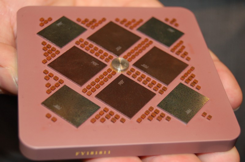 🇺🇸 United StatesPOWER5
Dual-core server microprocessor with simultaneous multithreadingCPU · Power · 2004
 🇺🇸 United States and 1 morePOWER7
IBM multi-core server processor from 2010CPU · Power · 2010
🇺🇸 United StatesIBM A2
Open source 64-bit Power ISA processor core for embedded systemsCPU · Power · 2010
 🇺🇸 United StatesPOWER3
64-bit PowerPC microprocessor for IBM workstations and serversCPU · Power · 1998
More from IBM
All of them 🇺🇸 United StatesCell Broadband Engine
A multi-core RISC processor pairing one PowerPC core with eight vector coprocessors.CPU · Power · 2007
 🇺🇸 United StatesBroadway
32-bit PowerPC CPU for the Nintendo Wii consoleCPU · Power · 2006
🇺🇸 United StatesKilocore
Multi-core processor with over 1,000 processing elementsCPU · Power · 2006
 WorldIBM z10
Quad-core mainframe processor from IBM released in 2008CPU · Other · 2008