
Intel 430HX
Socket 7 chipset for Pentium and MMX processors
The Intel 430HX, codenamed Triton II, is a chipset released in February 1996. It supports Socket 7 processors like the Pentium and Pentium MMX, offering features such as ECC memory support and symmetric multiprocessing.
- Released in February 1996 by Intel
- Supports up to 512MB of system RAM
- Includes ECC and parity RAM support
- Enables two-way symmetric multiprocessing
- Uses 82439HX northbridge and PIIX3 southbridge
What it is
The Intel 430HX is a computer chipset designed by Intel. Released in February 1996 under the codename Triton II, it serves as the bridge between the processor and other system components. This chipset supports Socket 7 processors, including the original Pentium, Pentium MMX, Cyrix 6x86, AMD K5, and AMD K6. Its official part number is 82430HX. It was notable for bringing server-grade features like error-correcting code memory support to desktop platforms.
How it came about
Intel launched the 430HX in February 1996 as an enhancement over its predecessor, the 430FX Triton I. The design aimed to improve system reliability and performance for high-end desktops and workstations. By integrating support for symmetric multiprocessing and parity checking, Intel targeted users who required greater data integrity and multi-processor capabilities within the Socket 7 ecosystem.
Inside the chip
The chipset comprises two main chips: the 82439HX TXC northbridge and the PIIX3 southbridge. It supports up to 512MB of random access memory, though cacheable memory depends on tag RAM size, ranging from 64MB to 512MB. Key architectural additions include support for error-correcting code and parity RAM, two-way symmetric multiprocessing, and universal serial bus connectivity. It also utilised peripheral component interconnect standards to boost data transfer speeds.
How it was made
Intel manufactured the 430HX chipset. The specific fabrication process node and transistor counts are not detailed in the available records. The physical implementation relies on the separate northbridge and southbridge configuration common to that era, rather than a single system-on-chip design.
Where it went
This chipset powered personal computers built around Socket 7 processors. It was suitable for systems using Intel Pentium and Pentium MMX CPUs, as well as compatible chips from AMD and Cyrix. The support for dual processors made it a choice for entry-level workstations requiring symmetric multiprocessing capabilities.
Versions and family
The 430HX succeeded the Intel 430FX. It was later replaced by the Intel 430VX and Intel 430TX chipsets. While the core design remained consistent, board implementations varied. Some motherboards did not allow tag RAM expansion, limiting cacheable memory to 64MB despite the chipset's higher theoretical limit.
Why it matters
The 430HX introduced robust memory management features to the mainstream PC market. By supporting error-correcting code and parity, it allowed desktop systems to achieve reliability levels previously reserved for servers. Its inclusion of universal serial bus support helped pave the way for broader adoption of that peripheral standard.
Problems and reception
The chipset had notable limitations. It did not support synchronous dynamic random access memory, which was emerging at the time. Additionally, dual-voltage support for newer processors like the Pentium MMX or AMD K6 was not mandatory on all boards. Users often needed an interposer to step down voltage for these CPUs, adding complexity to upgrades.
Questions people ask about Intel 430HX
Which processors does the Intel 430HX support?
It supports Socket 7 processors, including the Intel Pentium, Pentium MMX, Cyrix 6x86, AMD K5, and AMD K6. This broad compatibility made it a versatile choice for system builders during its release window.
What is the maximum memory capacity supported?
The chipset supports up to 512MB of RAM. However, the amount of cacheable memory varies between 64MB and 512MB, depending on the size of the tag RAM installed on the motherboard.
Does it support modern memory types like SDRAM?
No, the 430HX does not support synchronous dynamic random access memory technology. It was designed for earlier memory standards, which was a limitation as SDRAM began to emerge in the market.
What are the main components of this chipset?
It consists of two primary chips: the 82439HX TXC, which acts as the northbridge, and the PIIX3, which serves as the southbridge. This split design handles different system communication tasks.
Good reading and sources
The facts on this page come from the Wikipedia article "Intel 430HX", written by its contributors and used under the CC BY-SA 4.0 licence, and from its Wikidata record (CC0). EveryChip rewrote the text in its own words, with AI assistance, and compares every page with the article to make sure no passage is copied. It may be reused under the same CC BY-SA 4.0 licence with a link back.
It may contain mistakes, and figures change over time. Nothing here is investment or buying advice. If something is wrong, tell us. Last refreshed 2026-11-14.
Like Intel 430HX
All analog, power and mixed-signal WorldIntel 440FX
Chipset for Pentium Pro and early Pentium II processorsAnalog · 1996
 🇺🇸 United StatesPIIX
Intel southbridge family for x86 PCs from the mid-1990sAnalog · x86 · 1995
 🇺🇸 United StatesI/O Controller Hub
Intel southbridge chips managing motherboard data flowAnalog · 1999
🇺🇸 United StatesIntel X58
I/O hub for Nehalem processors with QuickPath InterconnectAnalog · 2008
More from Intel
All of them 🇺🇸 United StatesRDRAM
High-bandwidth serial memory developed by Rambus for PCs and consoles.Memory · 1996
🇺🇸 United StatesStrongARM
High-performance ARM microprocessor family for portable devicesCPU · Arm · 1996
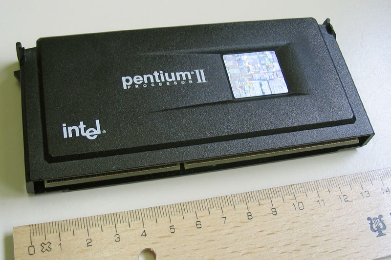 🇺🇸 United StatesPentium II
Intel's 1997 P6 desktop CPU line with MMX, sold in a slot cartridgeCPU · x86 · 1997
 🇺🇸 United StatesPentium Pro
Intel's first sixth-generation x86 CPU, built for servers and workstationsCPU · x86 · 1995