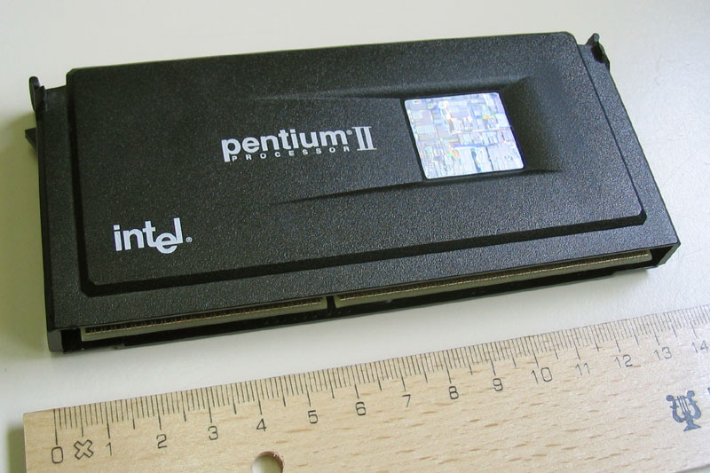
Pentium II
Intel's 1997 P6 desktop CPU line with MMX, sold in a slot cartridge
Pentium II is a family of sixth-generation x86 processors from Intel, first shipped on 7 May 1997 and built on the P6 design. It merged the Pentium Pro core with the MMX media instructions and ran from 233 to 450 MHz, staying in production for embedded use until the end of 2003.
- First P6 chip to carry the MMX integer SIMD instructions
- Level 2 cache lived on the cartridge and ran at half core speed
- Klamath: 350 nm, 7.5 million transistors, 233 to 300 MHz
- Dixon mobile core held 27.4 million transistors and 256 KB on-die cache
- Built from May 1997 until the end of 2003 for embedded use
What it is
Pentium II covers a line of Intel x86 microprocessors that began shipping in May 1997. It sits in the sixth generation of x86 chips and takes the P6 core design from the Pentium Pro, adding the MMX integer media instructions that had appeared on the Pentium MMX. Clock speeds across the family span 233 to 450 MHz, with front-side bus rates of 66 or 100 MT/s. Every model is a single-core part. The line was aimed at ordinary desktop buyers rather than the workstation market the Pentium Pro served, and it became the flagship of the Pentium name until the Pentium III arrived in February 1999.
How it came about
Intel built the Pentium II as a cheaper, more consumer-friendly follow-up to the Pentium Pro. Moving the level 2 cache off the processor die onto the cartridge solved the poor yields that had kept Pentium Pro prices high, so the new chip could be sold at mainstream prices. The first core, Klamath, reached shops on 7 May 1997. A shrunk core called Deschutes followed in January 1998, and mobile versions arrived from April 1998. In 1998 Intel also split the family, sending low-cost models to the Celeron name and server parts to Pentium II Xeon.
Inside the chip
The core is an improved P6 pipeline. Level 1 cache is 32 KB, split evenly between data and instructions, which is double the Pentium Pro figure. Four write buffers replace two, and either pipeline can use any of them. Segment register caches speed up 16-bit code, which mattered because much software of the day still used it, and an internal flag avoids needless pipeline flushes after partial register writes. Level 2 cache sits on the cartridge and ticks at half the core rate. It is always 512 KB and 16-way associative, against 4-way on the Pentium Pro. MMX adds packed integer SIMD operations.
How it was made
Klamath was built on Intel's 350 nm CMOS process with 7.5 million transistors. Deschutes and Tonga moved to 250 nm, cutting power draw; the Deschutes die measures 113 mm2. Dixon used 250 nm and, at 400 MHz, 180 nm, packing 27.4 million transistors on a 179.85 mm2 die. Most parts shipped as a plastic Slot 1 cartridge holding the CPU and its cache chips on a small board, with a heatsink clipped to one side. Later units switched to flip-chip packaging so the heatsink touched the die directly.
Where it went
Klamath systems first ran on the Intel 440FX Natoma chipset built for the Pentium Pro. Boards using the 440LX Balboa chipset then spread SDRAM and the AGP graphics slot. Deschutes at 100 MT/s paired with the 440BX Seattle family and its 440MX, 450NX and 440ZX relatives. Tonga and Dixon served notebook computers, while the Overdrive module let owners of Socket 8 Pentium Pro servers upgrade. Embedded versions kept being built until the close of 2003.
Versions and family
Klamath (80522) ran at 233, 266 and 300 MHz on a 66 MT/s bus. Deschutes (80523) covered 266 to 450 MHz and added FXSAVE and FXRSTOR for quick floating-point state handling. The Overdrive part combined a Deschutes core with a full-speed 512 KB cache in a Socket 8 module at 300 or 333 MHz. Tonga was the first mobile core. Dixon, sold as Pentium II PE, put 256 KB of full-speed cache on the die and reached 400 MHz. Xeon versions of Deschutes used Slot 2 and 512 KB, 1 MB or 2 MB of full-speed cache.
Why it matters
The cartridge approach let Intel place a large, cheap cache next to the core and still sell the chip to home buyers, which widened the reach of the P6 design. Boards around the 440LX and 440BX chipsets made SDRAM and AGP normal on desktop PCs. The family also set up the split that defined Intel's line-up for years: Celeron below, Xeon above. Its replacement, the Pentium III, differed mainly by adding SSE.
Problems and reception
One design limit drew comment. Klamath and early Deschutes parts carried a cache controller that could only track 512 MB of RAM, so systems with more memory ran slowly once past that point. A later revision, the 82459AD, raised the cacheable range to 4 GB. Some late Deschutes chips sold as 333 MHz were units locked to a 5 multiplier with the 100 MHz bus option turned off, and buyers found they would run well beyond 500 MHz when pushed.


Questions people ask about Pentium II
What kind of processor is the Pentium II?
It is a single-core x86 CPU from Intel, part of the sixth generation of that instruction set. The design is called P6 and it adds MMX media instructions to the Pentium Pro core. Clock speeds run from 233 to 450 MHz across the family.
Why did it come in a cartridge instead of a normal socket?
The plastic Slot 1 cartridge carried the processor and its level 2 cache chips on a small board. Keeping the cache off the die but close by let Intel avoid the low yields that had made the Pentium Pro expensive, while still offering 512 KB of cache.
How is its cache different from the Pentium Pro's?
The Pentium Pro had off-die cache running at full core speed. On the Pentium II the cache runs at half the core rate, but it is always 512 KB and 16-way associative rather than 4-way. Level 1 cache doubles to 32 KB to soften the slower level 2.
Which versions were made?
Desktop cores were Klamath and Deschutes, mobile cores were Tonga and Dixon, and a Socket 8 Overdrive module served Pentium Pro servers. Xeon variants of Deschutes used Slot 2 with up to 2 MB of full-speed cache, while Celeron covered the low end.
What replaced it?
The Pentium III took over as the flagship in February 1999. It was almost the same chip, with the addition of the SSE instruction set. Celeron carried on below it. Desktop Pentium II production ended in June 2001 and mobile parts in September 2001.
Good reading and sources
- Innovation starts hereIntel, Article
- Overclocking Special: The Intel Pentium II 300 SL2W8Tom's Hardware, Article
The facts on this page come from the Wikipedia article "Pentium II", written by its contributors and used under the CC BY-SA 4.0 licence, and from its Wikidata record (CC0). EveryChip rewrote the text in its own words, with AI assistance, and compares every page with the article to make sure no passage is copied. It may be reused under the same CC BY-SA 4.0 licence with a link back.
It may contain mistakes, and figures change over time. Nothing here is investment or buying advice. If something is wrong, tell us. Last refreshed 2026-11-14.
Like Pentium II
All CPUs and microprocessors 🇺🇸 United StatesXeon
Intel's x86 processor brand for servers, workstations and embedded systems since 1998CPU · x86 · 1998
 🇺🇸 United StatesP6
Intel's sixth x86 design, first with out-of-order executionCPU · x86 · 1995
 🇺🇸 United StatesIntel Core
Intel's multi-core x86 CPU line for laptops, desktops and workstationsCPU · x86 · 2006
 🇮🇱 IsraelIntel Core microarchitecture
Intel's 2006 multi-core CPU design that replaced NetBurst across desktops, laptops and serversCPU · x86 · 2006
More from Intel
All of them 🇺🇸 United StatesIntel740
1998 AGP graphics chip by Intel using system RAM for texturesGPU · 1998
 🇺🇸 United StatesCeleron
Intel's budget x86 desktop and mobile CPU line, sold from 1998 to 2023CPU · x86 · 1998
 🇺🇸 United StatesRDRAM
High-bandwidth serial memory developed by Rambus for PCs and consoles.Memory · 1996