
P6
Intel's sixth x86 design, first with out-of-order execution
P6 is the CPU microarchitecture Intel designed as the sixth major x86 generation, first shipping in the Pentium Pro of 1995. It powered the Pentium II and Pentium III lines and was prized for strong integer performance and low power draw, later evolving into Pentium M and Core.
- First Intel x86 core with out-of-order execution
- Debut: Pentium Pro, November 1995
- Pipeline stretched from 5 stages to 14
- 36-bit address bus, up to 64 GB of physical memory
- Pentium M drew a maximum of 27 W under load
What it is
P6 is a microarchitecture for Intel's Pentium-branded central processing units, the company's sixth major x86 design. It arrived in November 1995 inside the Pentium Pro and stayed in mainstream products through the Pentium III of 1999, with new P6-derived parts appearing into the mid-2000s. It was the first Intel x86 design to run instructions out of order, and it earned a reputation for frugal power use, strong integer work and a high instruction count per clock cycle. Later mobile designs, Pentium M and the Yonah Core chips, were modernised versions of the same basic core.
How it came about
The design began as the successor to the original Pentium, known as P5. Intel's engineers built a core that could translate x86 code into internal RISC-like micro-operations and reorder them, a technique NexGen had used earlier in the Nx586 of 1994. The Pentium Pro launched the approach in 1995. When NetBurst-based mobile chips proved too hot and inefficient for notebooks, Intel returned to the P6 blueprint and produced the Pentium M, then the Yonah core of January 2006 under the Core brand.
Inside the chip
Incoming IA-32 instructions are decoded into buffered micro-operations, which the core then reorders so several can be issued to execution units at once. Speculative and out-of-order execution, marketed as dynamic execution, needed new retire units and cut pipeline stalls. The pipeline grew from Pentium's 5 stages to 14 in the Pentium Pro, later trimmed for mobile parts. Other additions include register renaming, CMOV and FCMOV instructions, a 36-bit address bus with Physical Address Extension for 64 GB of memory, and a front-side bus letting four processors share resources. Pentium III added Streaming SIMD Extensions.
How it was made
Implementations spanned several process generations, starting at 500 nm with 5.5 million transistors and reaching 130 nm with 44 million. Intermediate steps included 350 nm, 250 nm and 180 nm. Chips were single-core and fitted Socket 8, Slot 1, Socket 370 or Socket 479. Intel manufactured the line in its own fabs.
Where it went
P6 cores powered the Pentium Pro, Pentium II, Pentium II Xeon, Pentium III and Pentium III Xeon, plus Celeron variants and a Pentium II Overdrive part for Socket 8. Mobile derivatives reached notebooks as Pentium M and Celeron M, and embedded designs such as the A100/A110, EP80579 and CE 3100. Server versions included Xeon LV and ULV (Sossaman).
Versions and family
The lineage runs from Pentium Pro through Pentium II and Pentium III, with Celeron budget siblings. The Pentium M branch (Banias, Dothan) enlarged caches to 64 KB L1 and up to 2 MB L2, added SSE2 and a 10- or 12-stage pipeline. The Enhanced Pentium M, Yonah, added SSE3, dual cores sharing 2 MB of L2 and a 667 MT/s bus. NetBurst partly replaced P6 in 2000, and the Core microarchitecture of July 2006 succeeded both.
Why it matters
P6 established out-of-order execution in Intel's x86 line and set the pattern for how x86 code is broken into internal micro-operations. Its efficiency made the Pentium M the leading notebook x86 chip for several years, able to challenge Mobile Pentium 4 parts running over 1 GHz faster. The Core microarchitecture that followed was derived from Enhanced Pentium M, and every later Intel design traces back to the Pentium Pro.
Problems and reception
One compatibility wrinkle affected early Pentium M chips: Banias supports PAE internally but does not set the PAE flag in CPUID. Some Linux distributions and Windows 8 or later refuse to boot on those processors because their kernels require the flag. Otherwise the family was well regarded for its balance of speed and power draw.
Questions people ask about P6
What is P6?
P6 is the name of the CPU design Intel used as its sixth generation of x86 processors. It first appeared in the Pentium Pro of 1995 and later ran the Pentium II and Pentium III families, along with mobile and server derivatives.
Why did P6 matter?
It was Intel's first x86 core to execute instructions out of order and to translate x86 code into internal micro-operations. That cut pipeline stalls and lifted instructions per clock, while keeping power use low enough for notebooks.
Which chips used it?
Pentium Pro, Pentium II, Pentium II Xeon, Pentium III, Pentium III Xeon and several Celeron lines, plus the Pentium M and Celeron M mobile families and embedded parts such as EP80579 and CE 3100.
What replaced it?
NetBurst, used in the Pentium 4 of 2000, partly took over. The Core microarchitecture launched on 27 July 2006 succeeded both, and was itself derived from the Enhanced Pentium M variant of P6.
Good reading and sources
The facts on this page come from the Wikipedia article "P6 (microarchitecture)", written by its contributors and used under the CC BY-SA 4.0 licence, and from its Wikidata record (CC0). EveryChip rewrote the text in its own words, with AI assistance, and compares every page with the article to make sure no passage is copied. It may be reused under the same CC BY-SA 4.0 licence with a link back.
It may contain mistakes, and figures change over time. Nothing here is investment or buying advice. If something is wrong, tell us. Last refreshed 2026-11-14.
Like P6
All CPUs and microprocessors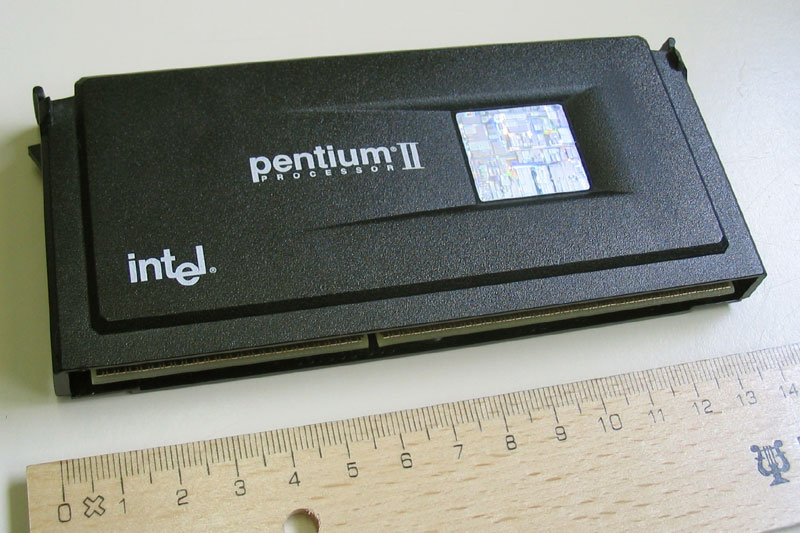 🇺🇸 United StatesPentium II
Intel's 1997 P6 desktop CPU line with MMX, sold in a slot cartridgeCPU · x86 · 1997
 🇺🇸 United StatesXeon
Intel's x86 processor brand for servers, workstations and embedded systems since 1998CPU · x86 · 1998
 🇺🇸 United StatesI386
First 32-bit x86 microprocessor by IntelCPU · x86 · 1985
 🇺🇸 United StatesIntel Core
Intel's multi-core x86 CPU line for laptops, desktops and workstationsCPU · x86 · 2006
More from Intel
All of them 🇺🇸 United StatesPentium Pro
Intel's first sixth-generation x86 CPU, built for servers and workstationsCPU · x86 · 1995
 🇺🇸 United StatesPentium OverDrive
Intel's mid-1990s upgrade chips for 486 and Pentium motherboardsCPU · x86 · 1995
 🇺🇸 United StatesPIIX
Intel southbridge family for x86 PCs from the mid-1990sAnalog · x86 · 1995
 🇺🇸 United StatesIntelDX4
Clock-tripled i486 CPU with 16 KB cache, at 75 or 100 MHzCPU · x86 · 1994