Programmable metallization cell
Non-volatile resistive memory using metal filaments
The programmable metallization cell (PMC) is a non-volatile memory technology developed at Arizona State University. It uses electrochemical reactions to form conductive filaments, offering an alternative to flash memory with lower power and higher density.
- Developed at Arizona State University in the 1990s
- Uses metal filaments to store data states
- Intrinsically radiation hard for space use
- Compatible with standard CMOS fabrication
- Offers lower power than flash memory
What it is
The programmable metallization cell, or PMC, is a type of non-volatile computer memory. Researchers at Arizona State University created it to serve as a potential successor to flash memory. The technology relies on changing resistance states within a tiny cell. It promises longer operational life, reduced power consumption, and greater storage density than traditional flash solutions. Companies like Infineon and Adesto have commercialised variants under names such as CBRAM.
How it came about
Professor Michael Kozicki led the development of this technology at Arizona State University during the 1990s. Early experiments used silver-doped germanium selenide glasses. Later work shifted to copper-doped electrolytes compatible with standard chip manufacturing. Axon Technologies was established in 1996 to bring the invention to market. Micron Technology and Infineon began collaborating on the project in the early 2000s. Adesto Technologies later licensed the rights and introduced a sample product in 2013.
Inside the chip
This memory type uses two metal electrodes separated by a solid electrolyte film. One electrode is inert, such as tungsten, while the other is active, like copper or silver. Applying a positive voltage causes metal ions to migrate and form a conductive filament. This creates a low-resistance state. Reversing the voltage dissolves the filament, returning the cell to a high-resistance state. The device reads data by measuring resistance without altering the filament structure.
How it was made
The cells can be built using materials compatible with standard CMOS fabrication processes. Copper-doped silicon-dioxide glass is one such material. This compatibility simplifies integration into existing semiconductor production lines. Theoretical scaling limits are extremely small, potentially reaching widths of just a few ions. A sample part with a capacity of 1 megabit was produced to demonstrate viability against EEPROM technologies.
Where it went
The primary application for this memory type is in space missions. Its structure makes it intrinsically resistant to radiation damage, a critical feature for satellites and probes. It also targets embedded systems where it can replace electrically erasable programmable read-only memory (EEPROM). The low power requirements and fast write speeds suit devices that need frequent data updates without the wear issues of flash memory.
Versions and family
Infineon Technologies refers to the technology as conductive-bridging RAM, or CBRAM. Adesto Technologies holds the registered trademark for this name. NEC developed a variant called Nanobridge, which uses copper sulphide or tantalum pentoxide. Sony calls their version electrolytic memory. These variations differ mainly in the specific electrolyte materials and electrode metals used to form the conductive paths.
Why it matters
PMC offers a solution to the physical degradation problems inherent in flash memory. Flash cells wear out after repeated writes due to high current requirements. This new approach uses low power and avoids the complex charge pumps needed by flash. It allows for simpler circuit layouts and potentially smaller feature sizes. The technology supports the continued miniaturisation of non-volatile storage beyond the limits of floating-gate transistors.
Questions people ask about Programmable metallization cell
How does a programmable metallization cell store data?
It stores data by forming or dissolving a tiny metallic filament between two electrodes. A conductive filament represents a low-resistance state, while its absence creates a high-resistance state. The device reads these resistance levels to determine the stored bit value.
Why is this memory suitable for space applications?
The technology is intrinsically radiation hard. Unlike flash memory, which can suffer data corruption or physical damage from high-energy particles in space, the electrochemical mechanism of PMC remains stable under radiation exposure.
What is the main advantage over flash memory?
PMC requires significantly less power to write data and does not degrade with use as quickly as flash. Flash memory suffers from limited write cycles due to physical wear, whereas PMC can endure many more operations without failure.
Good reading and sources
The facts on this page come from the Wikipedia article "Programmable metallization cell", written by its contributors and used under the CC BY-SA 4.0 licence, and from its Wikidata record (CC0). EveryChip rewrote the text in its own words, with AI assistance, and compares every page with the article to make sure no passage is copied. It may be reused under the same CC BY-SA 4.0 licence with a link back.
It may contain mistakes, and figures change over time. Nothing here is investment or buying advice. If something is wrong, tell us. Last refreshed 2026-11-14.
Like Programmable metallization cell
All memory chips WorldFerroelectric RAM
Non-volatile memory using ferroelectric capacitors for fast writes and low power.Memory
 World6264
JEDEC-standard 64 Kbit static RAM chipMemory
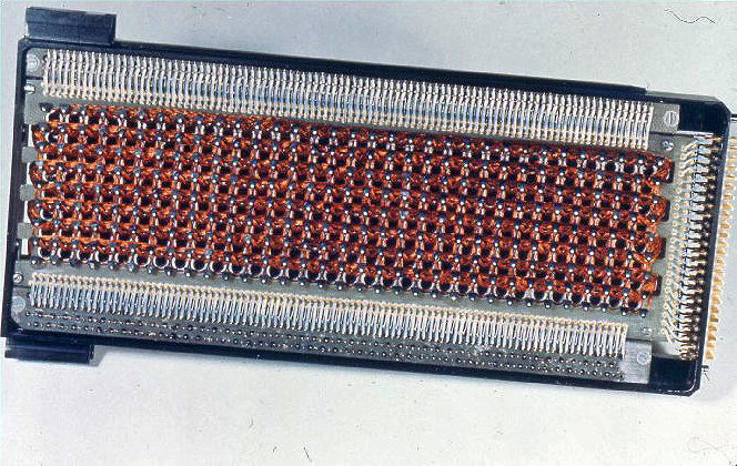 🇺🇸 United StatesCore rope memory
Read-only memory woven from magnetic cores and wireMemory
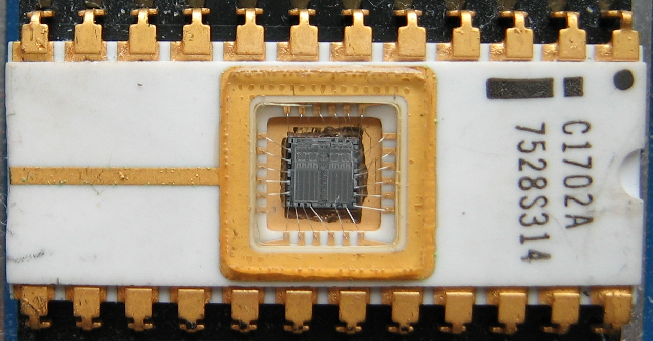 🇺🇸 United StatesEPROM
Non-volatile memory chip erased by ultraviolet lightMemory · 1971
More from Arizona State University
All of them 🇨🇦 CanadaXenos
Custom GPU for the Xbox 360 console by ATIGPU · GPU architecture
WorldQuad Data Rate SRAM
High-speed static memory with separate read and write busesMemory
 WorldDataFlash
Serial interface flash memory with SPI compatibilityMemory
 🇺🇸 United StatesIntel 8282
8-bit latch for Intel 8086 and 8080 systemsAnalog · Other