
Ferroelectric RAM
Non-volatile memory using ferroelectric capacitors for fast writes and low power.
Ferroelectric RAM is a non-volatile memory technology that uses a ferroelectric layer to store data without power. It offers faster write speeds and higher endurance than flash memory, though with lower storage density. Developed since the 1950s, it serves niche markets like smart cards and medical devices.
- Uses ferroelectric layer instead of dielectric for non-volatility
- Write endurance reaches 10^10 to 10^15 cycles
- Data retention exceeds 10 years at 85 degrees Celsius
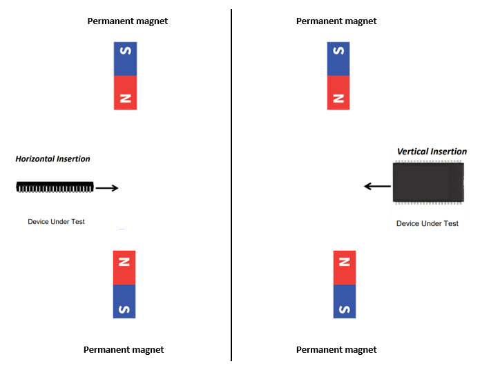
- Immune to strong magnetic fields up to 3700 gausses
- Write speeds under 150 ns compared to milliseconds for flash
What it is
Ferroelectric RAM, often called FeRAM or FRAM, is a type of random-access memory that retains data without power. It resembles dynamic RAM in structure but replaces the standard dielectric layer with a ferroelectric material, usually lead zirconate titanate. This change allows the chip to store binary states as electric polarizations rather than charge levels. The technology provides a reliable alternative to flash memory for applications requiring frequent writes and low energy consumption.
How it came about
MIT student Dudley Allen Buck first proposed the concept in his 1952 master’s thesis. Bell Telephone Laboratories experimented with ferroelectric crystals in 1955. Development accelerated in the late 1980s after MOS DRAM chips became common. NASA’s Jet Propulsion Laboratory explored non-destructive readout methods in 1991. Commercialization began in the mid-1990s, with Sega using the chips for game saves in 1994. Samsung and Hyundai Electronics introduced commercial products in 1996 and 1998 respectively.
Inside the chip
The storage cell uses one transistor and one capacitor, similar to DRAM. The capacitor contains a ferroelectric film where atoms shift polarity under an electric field. This shift creates a hysteresis loop, allowing two stable polarization states to represent binary zeros and ones. Reading data is destructive because it resets the polarization, so the system must rewrite the value immediately after reading. This architecture ensures data remains intact even during power loss or magnetic interference.
How it was made
Manufacturers produce FeRAM using complementary MOS processes. Early commercial chips used 500 nm nodes, while later devices utilized 350 nm and 130 nm lines. Fujitsu and Texas Instruments have operated production lines with FeRAM capability. Integrating these cells requires fewer masking steps than flash memory, simplifying embedding into microcontrollers. Recent research focuses on hafnium oxide materials to enable scaling below 10 nm and integration into advanced nodes.
Where it went
These chips appear in smart cards, radio-frequency identification tags, and utility meters due to their high write endurance. Medical devices such as portable dataloggers and implantable monitors use FeRAM for its low power draw. The automotive industry employs them in black boxes and airbag systems where rapid data saving is critical. Sony used embedded FeRAM in PlayStation 2 memory cards, and Sega utilized them for saving game progress in cartridges.
Versions and family
Standalone FeRAM chips exist alongside microcontrollers with embedded memory. Ramtron produced specialized chips for smart cards before being acquired by Cypress Semiconductor. Fujitsu manufactured both standalone and embedded versions. Modern prototypes aim for 9 to 16 megabit arrays with improved cycle counts. Research continues into vertical capacitor structures to increase density, addressing the limitation that smaller cells may lose their ferroelectric properties.
Why it matters
FeRAM occupies a small niche in the semiconductor market compared to flash memory. Its sales remain modest, with Ramtron reporting millions in revenue while flash generated billions. The technology proves valuable where flash fails, such as in high-endurance or low-power scenarios. It offers a viable solution for internet of things devices and industrial controls. However, higher costs and lower densities prevent it from replacing flash in mass storage applications.
Problems and reception
The technology faces challenges with imprint and fatigue, where previous writes affect future performance. Density limitations restrict its use in high-capacity storage. Despite these issues, it receives praise for reliability in magnetic fields and power efficiency. Manufacturers continue to refine the process to improve scalability and reduce production costs. Research institutions globally investigate new materials to overcome current physical limits.
Questions people ask about Ferroelectric RAM
How does FeRAM differ from standard DRAM?
FeRAM uses a ferroelectric material in its capacitor instead of a linear dielectric. This allows it to retain data without power, unlike DRAM which requires constant refreshing. The storage mechanism relies on atomic polarization rather than stored charge.
Why is FeRAM not used in large storage drives?
FeRAM has much lower storage density than flash memory. It cannot pack as many bits onto a single chip, making it significantly more expensive per bit. Flash technology also supports multiple bits per cell, further widening the cost gap.
What are the main advantages over flash memory?
FeRAM offers faster write speeds, lower power consumption, and vastly higher write endurance. It does not require high voltage charge pumps for writing, allowing operations to complete in nanoseconds rather than milliseconds.
Good reading and sources
- 1970: Semiconductors compete with magnetic cores | The Storage EngineComputer History Museum, Article
- Client ChallengeNature, Article
- Ferroelectric RAM on WikipediaEncyclopedia
- More photos on Wikimedia CommonsPhotos
- Wikidata recordOpen data
The facts on this page come from the Wikipedia article "Ferroelectric RAM", written by its contributors and used under the CC BY-SA 4.0 licence, and from its Wikidata record (CC0). EveryChip rewrote the text in its own words, with AI assistance, and compares every page with the article to make sure no passage is copied. It may be reused under the same CC BY-SA 4.0 licence with a link back.
It may contain mistakes, and figures change over time. Nothing here is investment or buying advice. If something is wrong, tell us. Last refreshed 2026-11-14.
Like Ferroelectric RAM
All memory chips World6264
JEDEC-standard 64 Kbit static RAM chipMemory
🇺🇸 United StatesProgrammable metallization cell
Non-volatile resistive memory using metal filamentsMemory
 🇺🇸 United StatesEPROM
Non-volatile memory chip erased by ultraviolet lightMemory · 1971
 🇺🇸 United States and 2 moreEEPROM
Byte-erasable non-volatile memory for small data storageMemory · 1978
More from Ramtron
All of them 🇺🇸 United StatesLM3914
Analog display driver for LED bar graphs and dot metersAnalog
 World78xx
Family of fixed positive linear voltage regulator integrated circuitsAnalog
🇰🇷 South KoreaISOCELL
Samsung family of CMOS image sensors for mobile and digital camerasSensor
 🇺🇸 United StatesLM386
Low-voltage audio power amplifier integrated circuitAnalog