
Charge-coupled device
Integrated circuit sensor that converts light into digital images.
Invented at Bell Labs in 1969, the charge-coupled device uses linked capacitors to capture light. It dominated high-quality imaging for decades before CMOS sensors replaced it in most consumer markets by the late 2010s.
- Invented by Willard Boyle and George E. Smith in 1969.
- Won the 2009 Nobel Prize in Physics for its creators.
- First used in a satellite imager in December 1976.
- Largely replaced by CMOS sensors in the late 2010s.
What it is
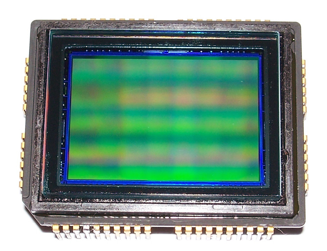
A charge-coupled device is an integrated circuit built from an array of linked capacitors. These components transfer electric charge under external control to read out data. In imaging applications, pixels act as metal-oxide-semiconductor capacitors that convert incoming photons into electron charges. This technology became a standard for professional, medical, and scientific imaging due to its high data quality. While active pixel sensors now dominate consumer electronics, CCDs remain vital where precision is critical.
How it came about
Willard Boyle and George E. Smith invented the concept at Bell Labs in 1969 while researching semiconductor memory. They realized electric charge could mimic magnetic bubbles and move across tiny capacitors. The first experimental device appeared in April 1970, demonstrating shift register capabilities. Fairchild Semiconductor soon produced commercial linear and two-dimensional devices. Sony later invested heavily to mass-produce these chips for camcorders, releasing the first consumer video camera in 1983. Boyle and Smith received the Nobel Prize in Physics in 2009 for this work.
Inside the chip
The sensor contains a photoactive silicon layer and a transmission region acting as a shift register. Light hits the capacitor array, generating charge proportional to intensity. A control circuit moves this charge from one capacitor to the next, like a bucket brigade. The final capacitor dumps its load into an amplifier, converting charge to voltage. Modern buried-channel designs keep charge away from the surface to reduce noise. Architectures vary between full-frame, frame-transfer, and interline types to manage shuttering and smear.
How it was made
Manufacturing starts with a lightly p-doped epitaxial silicon layer grown on a substrate. Phosphorus implantation creates n-doped channels for charge packets. Polysilicon gates are deposited and patterned using photolithography. Channel stops, made of thermally grown oxides, isolate columns to prevent charge mixing. These steps occur before gate formation to avoid heat damage. The process allows optimization for specific uses, such as reducing dark current or infrared response in interline-transfer devices.
Where it went
Early applications included memory and delay lines, but imaging quickly became the primary use. The KH-11 reconnaissance satellite launched in 1976 with an 800 by 800 pixel array. Consumer digital cameras adopted the technology after Steven Sasson built a still camera prototype in 1975. Sony popularized CCDs in camcorders during the 1980s. Today, they serve professional and scientific fields requiring high-quality data, though CMOS sensors have largely replaced them in general consumer electronics.
Versions and family
Architectures include full-frame, frame-transfer, and interline designs. Frame-transfer units use an opaque mask to store images quickly, reducing smear. Interline transfer devices further minimize smear from bright lights. The pinned photodiode, invented at NEC in 1980, solved early shutter lag issues by improving charge transfer. Color sensors emerged when Peter L. P. Dillon overlaid a filter array on a Fairchild chip in 1974. Peristaltic CCDs use additional implants to aid charge movement.
Why it matters
This invention revolutionized digital imaging, enabling everything from space telescopes to early digital cameras. It earned Willard Boyle and George E. Smith the 2009 Nobel Prize in Physics. Michael Tompsett received the National Medal of Technology and Innovation for his development work. The technology paved the way for modern digital photography and video recording. Although CMOS has taken over the mass market, the CCD established the foundation for electronic image capture.



Questions people ask about Charge-coupled device
How does a CCD capture an image?
Light hits an array of capacitors, creating electric charge proportional to brightness. A control circuit shifts this charge across the chip to an amplifier, which converts it into a voltage signal for digital processing.
Who invented the charge-coupled device?
Willard Boyle and George E. Smith at Bell Labs invented the concept in 1969. They were awarded the Nobel Prize in Physics in 2009 for this contribution to semiconductor technology.
Why are CMOS sensors more common now?
CMOS sensors have improved in quality while remaining cheaper and more power-efficient. By the late 2010s, they had largely replaced CCDs in consumer and professional digital cameras.
Good reading and sources
- L3CCD results in pure photon counting modearXiv, Article
- 1960: Metal Oxide Semiconductor (MOS) Transistor Demonstrated | The Silicon EngineComputer History Museum, Article
- Charge-coupled device on WikipediaEncyclopedia
- More photos on Wikimedia CommonsPhotos
- Wikidata recordOpen data
The facts on this page come from the Wikipedia article "Charge-coupled device", written by its contributors and used under the CC BY-SA 4.0 licence, and from its Wikidata record (CC0). EveryChip rewrote the text in its own words, with AI assistance, and compares every page with the article to make sure no passage is copied. It may be reused under the same CC BY-SA 4.0 licence with a link back.
It may contain mistakes, and figures change over time. Nothing here is investment or buying advice. If something is wrong, tell us. Last refreshed 2026-11-14.
Like Charge-coupled device
All image and other sensors 🇺🇸 United StatesQuantum well infrared photodetector
Infrared sensor using quantum wells for detectionSensor · 1987
 🇺🇸 United StatesMicrobolometer
Uncooled infrared sensor for thermal imaging camerasSensor · 1992
WorldStaring array
Two-dimensional image sensor for infrared and optical detectionSensor
 🇺🇸 United StatesDigital micromirror device
MEMS chip of tiny tilting mirrors that forms images in DLP projectorsSensor · Other · 1990
More from Bell Labs
All of them 🇺🇸 United StatesΜA741
Early monolithic operational amplifier with internal frequency compensationAnalog · 1968
🇺🇸 United StatesFour-Phase Systems AL1
An early 8-bit slice CPU built for Four-Phase's System IV/70 minicomputer.CPU · Other · 1970
 🇺🇸 United StatesBubble memory
Non-volatile magnetic storage using moving domains in thin filmsMemory · 1967
 🇯🇵 JapanNEC μCOM series
NEC microprocessor and microcontroller family from the 1970s and 1980sCPU · x86 · 1973