
POWER4
First dual-core non-embedded microprocessor from IBM
The POWER4 is a 64-bit microprocessor designed by IBM and released in 2001. It was the first non-embedded chip to place two processing cores on a single die, allowing RS/6000 and AS/400 servers to share hardware.
- First non-embedded chip with two cores on one die
- Released in 2001 by IBM for server use
- POWER4+ reached 1.9 GHz on 130 nm process
- Unified RS/6000 and AS/400 server lines
- Up to 128 MB L3 cache in multi-chip modules
What it is
The POWER4 is a microprocessor created by International Business Machines. It launched in 2001 as a 64-bit chip supporting PowerPC and PowerPC AS instruction sets. This design marked a major shift by placing two independent processing cores on one silicon die. It was the first time a non-embedded processor achieved this multicore layout. The chip allowed IBM to merge its RS/6000 and eServer iSeries product lines onto a common hardware platform.
How it came about
IBM developed the POWER4 to succeed the POWER3 and RS64 models. The primary goal was to converge two distinct server families into a single architecture. By supporting both RS/6000 and AS/400 systems, the company simplified its hardware offerings. The original version appeared in 2001 with speeds of 1.1 and 1.3 GHz. An enhanced model, the POWER4+, arrived in 2003 with higher clock rates and a smaller manufacturing process.
Inside the chip
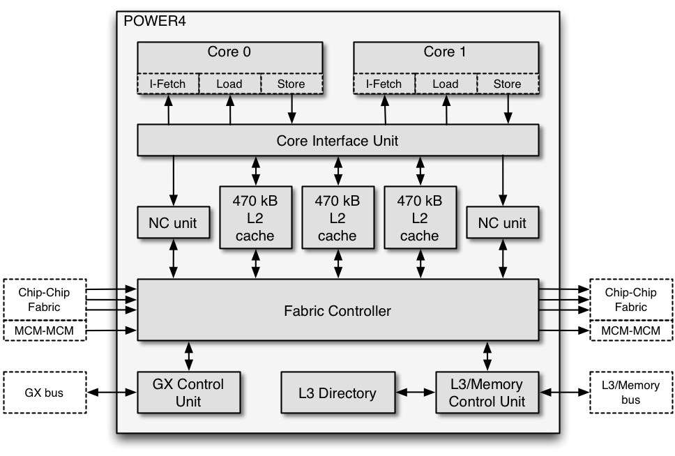
The chip uses a superscalar design with out-of-order execution. Eight independent units handle tasks, including two for floating-point math, two for loading data, and two for fixed-point calculations. A branch unit and conditional-register unit manage control flow. Each core has its own L1 cache, while a unified L2 cache is split into three parts. An off-chip L3 cache provides additional storage. The Fabric Controller manages communication between chips in larger systems.
How it was made
The initial POWER4 used a 180 nm process. The later POWER4+ shifted to a 130 nm silicon-on-insulator CMOS process with copper interconnects. This newer version contained 184 million transistors and measured 267 mm2. Packages could hold a single die or a multi-chip module with four dies. These modules supported up to 128 MB of shared error-correcting L3 cache.
Where it went
This processor powered high-end server systems. It ran in IBM RS/6000 machines and eServer iSeries models derived from the AS/400 line. The dual-core design enabled these servers to handle multiple workloads efficiently. It served as the foundation for the PowerPC 970, a derivative chip used in other computing applications. The architecture supported configurations with up to 32-way connectivity between chips.
Versions and family
The original POWER4 operated at 1.1 GHz and 1.3 GHz. The POWER4+ improved performance with speeds up to 1.9 GHz. Both versions featured two cores per die. The family included single-chip modules and multi-chip packages containing four dies. The PowerPC 970 is a notable derivative of this design. The POWER5 eventually succeeded the POWER4 series.
Why it matters
The POWER4 established the viability of multicore processors for enterprise servers. It was the first commercially available multiprocessor chip of its kind. By unifying IBM’s server lines, it reduced hardware complexity for large organisations. The design influenced subsequent generations of Power processors and demonstrated the benefits of integrating multiple cores on a single die.


Questions people ask about POWER4
What made the POWER4 unique when it launched?
It was the first non-embedded microprocessor to feature two processing cores on a single silicon die. This multicore design allowed it to handle more tasks simultaneously than previous single-core server chips.
Which computer systems used the POWER4 processor?
The chip powered IBM RS/6000 servers and eServer iSeries models. It enabled these two different product lines to run on the same hardware, helping IBM converge its server offerings.
How fast did the POWER4 and POWER4+ run?
The original POWER4 operated at clock speeds of 1.1 GHz and 1.3 GHz. The improved POWER4+ version increased this maximum speed to 1.9 GHz using a smaller 130 nm manufacturing process.
Good reading and sources
The facts on this page come from the Wikipedia article "POWER4", written by its contributors and used under the CC BY-SA 4.0 licence, and from its Wikidata record (CC0). EveryChip rewrote the text in its own words, with AI assistance, and compares every page with the article to make sure no passage is copied. It may be reused under the same CC BY-SA 4.0 licence with a link back.
It may contain mistakes, and figures change over time. Nothing here is investment or buying advice. If something is wrong, tell us. Last refreshed 2026-11-14.
Like POWER4
All CPUs and microprocessors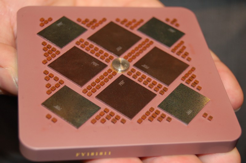 🇺🇸 United StatesPOWER5
Dual-core server microprocessor with simultaneous multithreadingCPU · Power · 2004
 🇺🇸 United StatesPOWER3
64-bit PowerPC microprocessor for IBM workstations and serversCPU · Power · 1998
 🇺🇸 United StatesIBM RS64
64-bit microprocessor family for IBM commercial serversCPU · Power · 1997
 WorldPOWER6
Dual-core IBM server microprocessor with hardware decimal mathCPU · Power · 2007
More from IBM
All of them 🇺🇸 United StatesRAD750
Radiation-hardened PowerPC processor for spacecraft and satellitesCPU · Power · 2001
 🇺🇸 United StatesPowerPC 970
IBM's 64-bit PowerPC desktop CPU family, sold by Apple as the G5.CPU · Power · 2002
 🇺🇸 United StatesGekko
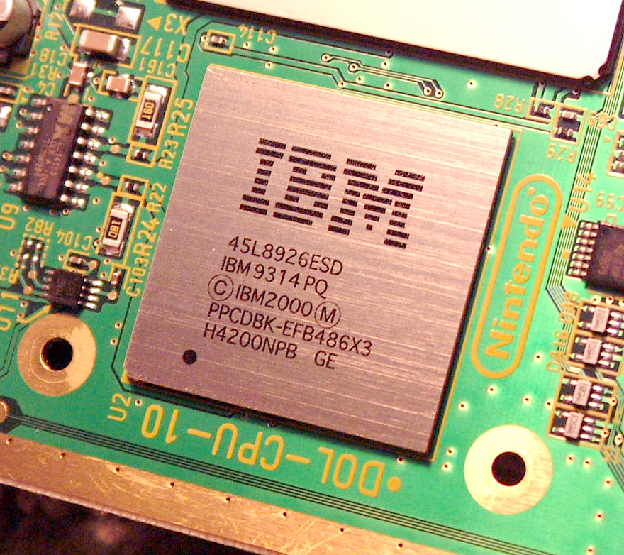
Custom PowerPC CPU for the Nintendo GameCubeCPU · Power · 2000
🇺🇸 United StatesAlpha 21364
DEC microprocessor with integrated memory and network controllersCPU · 2002