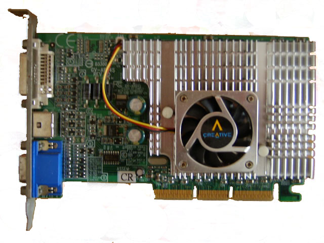
Radeon R100
First generation Radeon graphics chip with hardware T&L
ATI Technologies launched the Radeon R100 in April 2000 as its first DirectX 7 compatible GPU. It introduced hardware transform and lighting to offload geometry tasks from the CPU, marking a major step up from the older Rage series.
- Launched in April 2000 by ATI Technologies
- Built on a 180 nm process by TSMC
- Introduced HyperZ for memory optimization
- Features hardware transform and lighting engine
- Supports Direct3D 7.0 and OpenGL 1.3
What it is
The Radeon R100 is the first graphics processing unit in the Radeon line from ATI Technologies. Released in spring 2000, it brought hardware transform and lighting to the consumer market. This feature allowed the chip to handle complex geometry calculations itself, rather than relying on the main computer processor. The design supported Direct3D 7.0 and OpenGL 1.3, offering better 3D acceleration than the preceding Rage series. It also included tools for video acceleration and multiple display outputs.
How it came about
ATI developed the R100 to compete with the Nvidia GeForce 256, as their older Rage 128 Pro could not keep up. Early marketing materials referred to the card as the Radeon 256, likely to draw direct comparisons with the rival product. The final name dropped this number. The chip was code-named Rage 6 during development. It launched in April 2000, aiming to provide a modern feature set for PC gamers and professionals who needed faster 3D rendering capabilities.
Inside the chip
The architecture uses a dual-pipeline design, often called a 2x3 configuration. Each of the two pipelines can process three texture maps per pixel every clock cycle. This setup allowed for advanced effects like environment mapped bump mapping. A key innovation was HyperZ, a technology that reduced overdraw and optimized memory bandwidth usage. While the chip had programmable shading elements, it did not support the Pixel Shader 1.0 or 1.1 standards defined in DirectX 8.0.
How it was made
TSMC manufactured the R100 using a 180 nanometre process. The initial die contained 30 million transistors. The reference design ran the core at 183 MHz, paired with DDR memory clocked at the same speed. Later variants, such as the RV200 used in the Radeon 7500, moved to a smaller 150 nm process. This shrink allowed for higher clock speeds and asynchronous operation between the core and memory, improving overall efficiency and performance potential.
Where it went
These chips powered desktop graphics cards for personal computers. They were common in gaming rigs and workstations requiring 3D acceleration. The RV100 variant, sold as the Radeon VE or 7000, found use in budget systems and notebooks under the Mobility Radeon brand. Integrated graphics versions, known as the 3xx series IGPs, appeared on motherboards for AMD and Intel processors, providing basic display capabilities for office and home PCs.
Versions and family
The original R100 shipped as the Radeon DDR and a slower SDR version. An OEM-only LE model used bins that failed full specifications, disabling HyperZ by default. In 2001, ATI rebranded the line as the Radeon 7200. The RV100 cut features for the entry-level Radeon 7000, removing hardware T&L but adding dual-monitor support. The RV200 refreshed the design for the Radeon 7500, offering higher clocks and better efficiency while retaining the core architecture.
Why it matters
The R100 established the foundation for the long-running Radeon brand. Its HyperZ technology became a standard approach for managing memory bandwidth in subsequent graphics chips. Although it trailed the GeForce2 in some 16-bit benchmarks, it competed well in 32-bit colour modes. The introduction of hardware T&L marked a shift in how PCs handled 3D geometry, freeing up the central processor for other tasks and enabling more complex scenes in games.
Problems and reception
Reviewers noted that the card performed below the GeForce2 GTS in many tests, particularly at lower colour depths. However, it offered superior image quality and feature completeness in areas like bump mapping. The lack of official DirectX 8 pixel shader support was a point of confusion, though ATI explained that the hardware could achieve similar results through other means. The budget VE model struggled in 3D performance but excelled in multi-display setups.


Questions people ask about Radeon R100
Does the Radeon R100 support pixel shaders?
No, it does not support DirectX 8.0 Pixel Shader 1.0 or 1.1. While it has programmable elements, the silicon cannot execute these specific shader models. ATI stated that developers could achieve similar effects using extended multitexture capabilities instead.
What is HyperZ technology?
HyperZ is a memory bandwidth optimization feature introduced with the R100. It reduces overdraw and improves the efficiency of 3D rendering by culling hidden pixels before they are processed, allowing the card to compete with faster rivals.
How does the R100 compare to the GeForce 256?
The R100 was designed to compete with the GeForce 256. It offered similar hardware transform and lighting capabilities. In benchmarks, it often trailed the GeForce2 in 16-bit colour but could match or beat it in 32-bit colour modes due to its efficient architecture.
Good reading and sources
- Radeon R100 series on WikipediaEncyclopedia
- More photos on Wikimedia CommonsPhotos
- Wikidata recordOpen data
The facts on this page come from the Wikipedia article "Radeon R100 series", written by its contributors and used under the CC BY-SA 4.0 licence, and from its Wikidata record (CC0). EveryChip rewrote the text in its own words, with AI assistance, and compares every page with the article to make sure no passage is copied. It may be reused under the same CC BY-SA 4.0 licence with a link back.
It may contain mistakes, and figures change over time. Nothing here is investment or buying advice. If something is wrong, tell us. Last refreshed 2026-11-14.
Like Radeon R100
All graphics processors WorldGeForce 3 series
Third-generation Nvidia GPU with programmable shadersGPU · GPU architecture · 2001
 WorldGeForce 256
Nvidia's first GeForce, a 1999 3D accelerator with hardware transform and lightingGPU · GPU architecture · 1999
 🇺🇸 United StatesGeForce
Nvidia brand of graphics processing units for PC gaming and computing.GPU · GPU architecture · 1999
 WorldGeForce 4 series
Fourth generation of Nvidia GeForce graphics processorsGPU · GPU architecture · 2002
More from ATI Technologies
All of them 🇨🇦 CanadaRadeon R200
Second-generation ATI GPU with DirectX 8.1 supportGPU · GPU architecture · 2001
 🇨🇦 CanadaRadeon R300
First consumer GPU with full Direct3D 9 supportGPU · GPU architecture · 2002
 🇨🇦 CanadaR420
ATI GPU core for Radeon X800 graphics cardsGPU · GPU architecture · 2004