
POWER2
IBM RISC processor for RS/6000 workstations
The POWER2 is a central processing unit designed by IBM and released in September 1993. It implemented the POWER instruction set architecture and served as the successor to the POWER1 chip. Initially the fastest microprocessor available, it powered high-end RS/6000 systems before being succeeded by the POWER3.
- Debuted in September 1993 as the fastest microprocessor
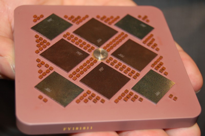
- Used a multi-chip module with up to eight dies
- Manufactured on a 0.72 micron CMOS process
- Powered the IBM Deep Blue supercomputer nodes
- Succeeded by the single-chip POWER2 Super Chip
What it is
The POWER2 is a reduced instruction set computer processor created by IBM. It launched in September 1993 as part of the RS/6000 product line. This chip succeeded the earlier POWER1 design and implemented the POWER instruction set architecture. At its debut, it held the title of the fastest microprocessor on the market, briefly outperforming the Alpha 21064. The design focused on high performance for technical computing tasks through enhanced instruction sets and higher clock speeds.
How it came about
IBM developed the POWER2 to replace the POWER1, originally calling the project RIOS2. The team aimed to improve upon the previous generation by adding new system instructions and increasing operating frequencies. When it arrived in late 1993, it claimed the performance lead in the industry. However, this advantage was short-lived, as the updated Alpha 21064A arrived later that same year and took the top spot. The compiler support for this architecture was eventually dropped in GCC version 4.5.
Inside the chip
The processor uses a multi-chip module approach rather than a single die. Depending on the cache size, the design uses six or eight semi-custom integrated circuits. These include separate units for instruction caching, fixed-point math, floating-point calculations, storage control, and data caching. The eight-chip version features a 32 KB instruction cache and up to 256 KB of data cache. An extra fixed-point unit and floating-point unit were added compared to the predecessor. The memory bus and cache structures were optimized for high throughput in scientific workloads.
How it was made
IBM manufactured the chips using a 0.72 micron CMOS process with an effective channel length of 0.45 microns. The fabrication involved one layer of polysilicon and four layers of metal interconnect. The eight-chip configuration contains 23 million transistors spread across a total die area of 1,215 square millimetres. These individual dies are packaged together in a ceramic multi-chip module measuring 64 mm by 64 mm. This packaging method allowed IBM to combine multiple specialized units into a single processor package.
Where it went
The primary application for the POWER2 was in IBM RS/6000 systems, which served as high-performance workstations and servers. Its floating-point capabilities made it suitable for technical computing and engineering simulations. The later P2SC variant, a single-chip version, was used in the IBM Deep Blue supercomputer. Although Deep Blue is famous for defeating chess champion Garry Kasparov, its chess logic ran on custom VLSI chips, not the general-purpose P2SC processors.
Versions and family
IBM released the POWER2+ in May 1994, optimizing it for transaction processing. This version added off-package L2 cache options ranging from 512 KB to 2 MB and used a smaller solder ball connect package to reduce costs. The POWER2 Super Chip, or P2SC, arrived in October 1996. It integrated the eight-chip design onto a single die using a 0.29 micron process. The P2SC ran at up to 135 MHz but halved the L1 data cache capacity to fit the design. A faster 160 MHz version followed in 1997.
Why it matters
The POWER2 demonstrated IBM's ability to deliver high-performance RISC processors during the early 1990s. It briefly held the title of the world's fastest microprocessor, showcasing strong floating-point performance. The transition from a multi-chip module to the single-chip P2SC illustrated the rapid advances in semiconductor manufacturing density. This lineage continued with the POWER3, which became the flagship processor for the RS/6000 line in 1998.


Questions people ask about POWER2
What was the original name of the POWER2?
The processor was originally named RIOS2 during its development phase. IBM later marketed it as the POWER2 when it launched in September 1993 as part of the RS/6000 family.
How many chips make up a POWER2 processor?
The POWER2 uses a multi-chip design consisting of either six or eight semi-custom integrated circuits. The eight-chip configuration is required for models with the larger 256 KB data cache.
Did the POWER2 run the Deep Blue chess computer?
The P2SC variant of the POWER2 was used in the Deep Blue supercomputer nodes. However, the actual chess-playing intelligence came from custom VLSI chips, not the general-purpose POWER2 processors.
Good reading and sources
The facts on this page come from the Wikipedia article "POWER2", written by its contributors and used under the CC BY-SA 4.0 licence, and from its Wikidata record (CC0). EveryChip rewrote the text in its own words, with AI assistance, and compares every page with the article to make sure no passage is copied. It may be reused under the same CC BY-SA 4.0 licence with a link back.
It may contain mistakes, and figures change over time. Nothing here is investment or buying advice. If something is wrong, tell us. Last refreshed 2026-11-14.
Like POWER2
All CPUs and microprocessors 🇺🇸 United StatesIBM Power
RISC microprocessors for servers and supercomputers by IBMCPU · Power · 1990
 🇺🇸 United StatesPOWER3
64-bit PowerPC microprocessor for IBM workstations and serversCPU · Power · 1998
 🇺🇸 United StatesPOWER5
Dual-core server microprocessor with simultaneous multithreadingCPU · Power · 2004
 WorldPOWER6
Dual-core IBM server microprocessor with hardware decimal mathCPU · Power · 2007
More from IBM
All of them 🇺🇸 United StatesPowerPC 600
Early PowerPC processor family for PCs, workstations and embedded gearCPU · Power · 1993
 🇺🇸 United StatesCyrix Cx486
x86 desktop microprocessor competing with Intel 486CPU · x86 · 1993
 🇺🇸 United States and 1 moreMwave
IBM digital signal processor for combined audio and telephonyDSP · Other · 1992
 🇺🇸 United StatesPowerPC 400
Embedded 32-bit RISC processor cores for diverse applicationsCPU · Power · 1994