
AMD K6-III
x86 desktop processor with on-die L2 cache
The AMD K6-III is an x86 microprocessor launched in February 1999. It integrated 256 KB of L2 cache on the die, boosting integer performance against Intel rivals. This chip was the final desktop CPU for Socket 7 before the Athlon era.
- First AMD chip with 256 KB on-die L2 cache
- Last desktop processor for Socket 7 platform
- Recalled 500 MHz model due to high current draw
- Mobile variants supported PowerNow! energy saving
What it is
The K6-III is a single-core x86 microprocessor developed by AMD. Released in early 1999, it served as a high-performance option for desktop computers using Socket 7 or Super Socket 7 motherboards. Its primary innovation was moving the secondary cache onto the processor die. This change significantly improved data access speeds compared to earlier models that relied on slower motherboard-mounted cache. The chip competed directly with Intel Pentium II and early Pentium III processors during its short market life.
How it came about
AMD designed the K6-III to extend the life of the Socket 7 platform. The team built upon the existing K6-2 architecture but added a substantial on-die cache. Launching in February 1999, the 450 MHz model quickly gained recognition for its strong integer performance. However, manufacturing challenges at higher frequencies limited its lifespan. AMD recalled the rare 500 MHz version due to excessive current draw that risked damaging motherboards. The company soon shifted focus to the new Athlon line, ending K6-III production to free up factory capacity.
Inside the chip
This processor uses the K6 microarchitecture with a short six-stage pipeline. It contains 21.4 million transistors on a die measuring 118 square millimetres. The design features 64 KiB of level one cache split into data and instructions. A key feature is the 256 KiB of full-speed level two cache located on the die. This setup enabled AMD's TriLevel Cache scheme, where the external motherboard cache acted as a third-level cache. The chip supports MMX and 3DNow! instruction sets for multimedia tasks, though its floating-point unit lagged behind Intel competitors in gaming.
How it was made
Initial models were manufactured using a 250 nanometre process. Later mobile variants, known as K6-III+ and K6-2+, used a shrunk 180 nanometre process. These newer versions included PowerNow! technology for energy savings. The original desktop chips required careful voltage regulation, operating at 2.2 V or 2.4 V. Production costs were higher than the simpler K6-2 due to the larger die size and complex cache structure. AMD eventually ceased production to prioritise the more profitable Athlon processors.
Where it went
The K6-III powered desktop personal computers during the late 1990s. It offered a cost-effective upgrade path for users with existing Socket 7 systems. While intended for desktops, the later low-power K6-III+ and K6-2+ models targeted mobile laptops. Enthusiasts also adopted these mobile chips for desktop use, often modifying BIOS settings to support them. Overclockers favoured these variants for their ability to run at speeds beyond official ratings, despite the architectural limits on frequency scaling.
Versions and family
The family includes the standard desktop K6-III and the mobile K6-III-P. The K6-III+ and K6-2+ are refined versions made on a smaller process node. The K6-2+ has half the L2 cache of the K6-III+ but shares the same core design. Clock speeds ranged from 333 MHz to 550 MHz for desktop parts, with mobile versions reaching up to 570 MHz unofficially. The K6-III+ introduced Enhanced 3DNow! instructions, adding digital signal processing capabilities not present in the original model.
Why it matters
The K6-III demonstrated that on-die cache could deliver high performance on older platforms. It held the title of fastest x86 processor for integer tasks upon launch. However, its inability to scale past 500 MHz highlighted the limits of the K6 architecture. The chip helped bridge the gap until the Athlon arrived, maintaining AMD's presence in the market. Its legacy persists among retro computing enthusiasts who value its role in the evolution of cache hierarchy designs.
Problems and reception
Reviewers praised the integer speed of the 450 MHz model but noted weaknesses in floating-point gaming performance. The recall of the 500 MHz unit damaged confidence in high-frequency stability. Supply issues made the chip difficult to obtain as AMD prioritised Athlon production. Despite this, the mobile variants found a loyal following among overclockers who achieved speeds near 800 MHz with air cooling. The lack of motherboard support for high front-side bus speeds remained a bottleneck for extreme tuning.


Questions people ask about AMD K6-III
What makes the K6-III different from the K6-2?
The main difference is the location of the L2 cache. The K6-III places 256 KB of cache directly on the processor die, running at full clock speed. The K6-2 relies on slower cache mounted on the motherboard. This change greatly improves data access times and overall system responsiveness.
Can I use a K6-III+ in a standard desktop PC?
Yes, but it may require a BIOS update. The K6-III+ was designed for laptops, so many desktop motherboards do not support it officially. Enthusiasts often use unofficial BIOS patches to enable these chips on older Socket 7 boards, allowing for lower power usage and overclocking potential.
Why was the 500 MHz K6-III recalled?
AMD recalled the 500 MHz version because it drew too much electrical current. This excessive power draw posed a risk of damaging the motherboards it was installed in. As a result, AMD stopped selling speeds above 450 MHz and focused on developing the next-generation Athlon processor instead.
Good reading and sources
- Socket 7: Fit For Years To Come!Tom's Hardware, Article
- AMD to kill K6, K6-II, K6-IIIThe Register, Article
The facts on this page come from the Wikipedia article "AMD K6-III", written by its contributors and used under the CC BY-SA 4.0 licence, and from its Wikidata record (CC0). EveryChip rewrote the text in its own words, with AI assistance, and compares every page with the article to make sure no passage is copied. It may be reused under the same CC BY-SA 4.0 licence with a link back.
It may contain mistakes, and figures change over time. Nothing here is investment or buying advice. If something is wrong, tell us. Last refreshed 2026-11-14.
Like AMD K6-III
All CPUs and microprocessors 🇺🇸 United StatesAthlon
AMD's x86 desktop processor brand, from the first 1 GHz chip to entry-level Zen APUsCPU · x86 · 1999
 🇺🇸 United StatesPentium III
Intel's 32-bit P6 desktop and server CPU line, launched in 1999 with SSE.CPU · x86 · 1999
 🇺🇸 United StatesXeon
Intel's x86 processor brand for servers, workstations and embedded systems since 1998CPU · x86 · 1998
 🇺🇸 United StatesK6-2
x86 microprocessor with 3DNow! instructions for budget PCsCPU · x86 · 1998
More from AMD
All of them 🇺🇸 United StatesGeode
Low-power x86 system-on-chip for embedded devicesSoC · x86 · 1999
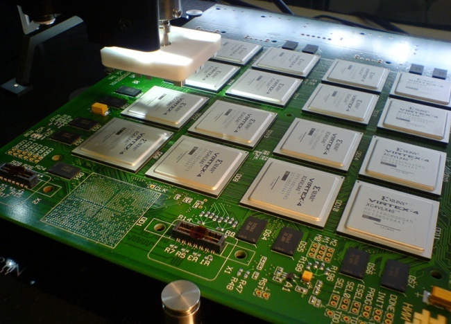 🇺🇸 United StatesVirtex
High-performance FPGA family by AMD and XilinxFPGA · Other · 1999
🇺🇸 United StatesRadeon
Brand of graphics processors and computer products by AMDGPU · GPU architecture · 2000
🇺🇸 United StatesAlchemy
Ultra low power MIPS embedded microprocessor familySoC · MIPS · 2000