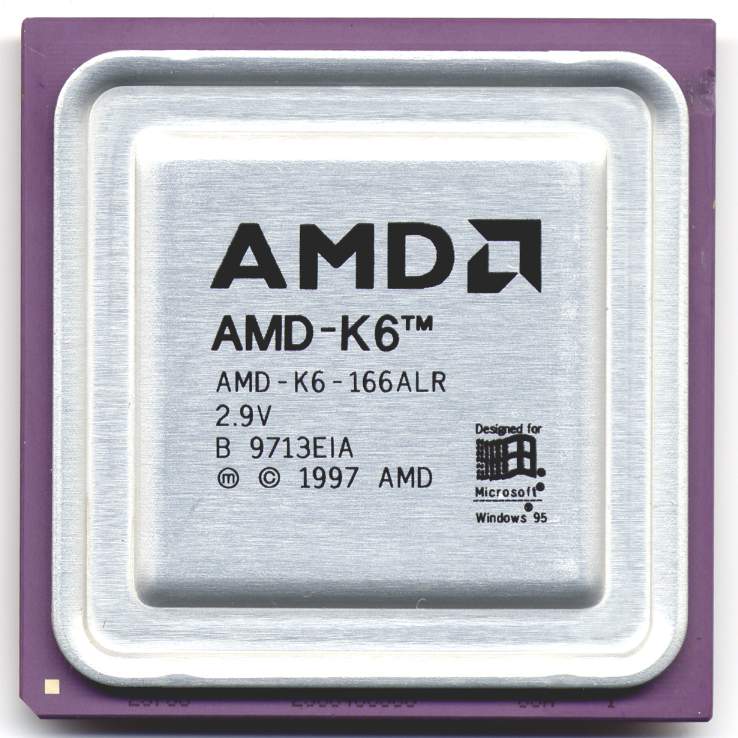
AMD K6
x86 microprocessor for Socket 7 desktops
The AMD K6 is a single-core x86 microprocessor launched in April 1997. Designed by the former NexGen team, it offered Pentium II-level performance at a lower cost and fit existing Socket 7 motherboards.
- Launched in April 1997 for Socket 7 systems
- Based on NexGen Nx686 design acquired by AMD
- Shrunk from 350 nm to 250 nm process node
- Reached peak speed of 300 MHz in May 1998
- Included 64 KiB L1 cache and MMX support
What it is
The AMD K6 is a discontinued microprocessor that entered the market in 1997. It serves as a central processing unit for personal computers, designed to compete directly with Intel offerings. The chip fits into standard Socket 7 motherboards, allowing users to upgrade older systems without replacing the entire board. AMD marketed it as a cost-effective alternative to the Pentium II, delivering similar performance for less money. This strategy helped AMD gain significant share in the desktop PC sector during the late 1990s.
How it came about
Although named to suggest evolution from the AMD K5, the K6 architecture originated from NexGen. AMD acquired NexGen and its Nx686 design, adapting it for mass production. Chief architect Greg Favor led the team that integrated this new core. The first models launched in April 1997 at 166 and 200 MHz. AMD initially used a performance rating system but later switched to actual clock speeds. The design evolved quickly, moving from a 350 nm process to a smaller 250 nm node in 1998, enabling higher frequencies up to 300 MHz.
Inside the chip
The K6 uses a superscalar design with seven execution units for parallel instruction handling. It translates x86 assembly code into internal RISC86 micro-operations on the fly. This dynamic buffering allows for out-of-order execution and speculative optimization. The processor includes a floating-point unit and supports MMX instructions for multimedia tasks. It features register renaming to improve pipeline efficiency. The L1 cache holds 64 KiB, split evenly between data and instructions. Boundary scan support follows the IEEE 1149.1 standard for testing.
How it was made
AMD manufactured the K6 using two different process nodes. The initial Model 6 chips used a 350 nm process and contained 8.8 million transistors. These ran at voltages between 2.9 and 3.3 V. In January 1998, AMD introduced the Model 7, codenamed Little Foot. This version shrank the die to 250 nm, reducing power needs to 2.2 V. The smaller geometry allowed for higher clock speeds, reaching up to 300 MHz by May 1998. Both versions maintained pin compatibility with Socket 7 standards.
Where it went
This processor targeted the mainstream desktop PC market. Its primary advantage was backward compatibility with existing Socket 7 motherboards. Users could upgrade from earlier Pentium or K5 systems without buying new memory or peripherals. The chip handled general computing tasks, office applications, and early multimedia workloads via MMX extensions. It provided a viable budget option for consumers who wanted near-Pentium II performance without the high cost of new Intel platforms.
Versions and family
The K6 line began with Model 6, running at 166, 200, and 233 MHz. Model 7, known as Little Foot, expanded the range to include 266 and 300 MHz variants. The 266 MHz model required specific motherboard support due to voltage and multiplier changes. AMD eventually replaced the standard K6 with the K6-2, which added 3DNow! instructions for enhanced 3D graphics performance. The K6-2 succeeded the original design in May 1998.
Why it matters
The K6 challenged Intel's dominance in the x86 processor market. By offering competitive speed at a lower price point, it forced Intel to adjust its pricing strategies. The chip demonstrated that AMD could produce high-performance designs through strategic acquisitions like NexGen. It established a foundation for future AMD processors, proving the viability of their independent architectural development. The success of the K6 series helped stabilize AMD's financial position during a competitive era.
Problems and reception
Reviews at launch highlighted the K6 as a fast and affordable option. Some reports claimed it was the fastest x86 chip available at the time. However, compatibility issues arose with the later 266 MHz and 300 MHz models on older Socket 7 boards. Users needed to verify motherboard support for the lower voltage requirements. Despite these minor hurdles, the processor was well-received for its value proposition and performance relative to cost.


Questions people ask about AMD K6
What socket does the AMD K6 use?
The AMD K6 uses Socket 7. This design allows it to fit into many existing motherboards built for Intel Pentium processors, making upgrades easier for users with older systems.
How many transistors are in the K6?
Both the original Model 6 and the later Little Foot Model 7 contain 8.8 million transistors. The count remained the same even as the manufacturing process shrunk from 350 nm to 250 nm.
What is the difference between K6 Model 6 and Model 7?
Model 6 used a 350 nm process with higher voltages. Model 7, called Little Foot, used a 250 nm process, ran at 2.2 V, and supported higher clock speeds up to 300 MHz.
Did the K6 support MMX instructions?
Yes, the K6 included support for MMX instructions. These extensions helped improve performance for multimedia applications such as audio and video processing on personal computers.
Good reading and sources
The facts on this page come from the Wikipedia article "AMD K6", written by its contributors and used under the CC BY-SA 4.0 licence, and from its Wikidata record (CC0). EveryChip rewrote the text in its own words, with AI assistance, and compares every page with the article to make sure no passage is copied. It may be reused under the same CC BY-SA 4.0 licence with a link back.
It may contain mistakes, and figures change over time. Nothing here is investment or buying advice. If something is wrong, tell us. Last refreshed 2026-11-14.
Like AMD K6
All CPUs and microprocessors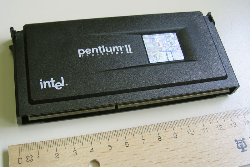 🇺🇸 United StatesPentium II
Intel's 1997 P6 desktop CPU line with MMX, sold in a slot cartridgeCPU · x86 · 1997
 🇺🇸 United StatesMediaGX
Integrated x86 system on a chip for low-cost PCsSoC · x86 · 1997
 🇺🇸 United StatesWinChip
Low-power x86 processor for Socket 7 systemsCPU · x86 · 1997
 🇺🇸 United StatesXeon
Intel's x86 processor brand for servers, workstations and embedded systems since 1998CPU · x86 · 1998
More from AMD
All of them 🇺🇸 United StatesAMD K5
AMD's first in-house x86 microprocessor for desktop PCsCPU · x86 · 1996
 🇺🇸 United StatesK6-2
x86 microprocessor with 3DNow! instructions for budget PCsCPU · x86 · 1998
 🇺🇸 United StatesAMD K6-III
x86 desktop processor with on-die L2 cacheCPU · x86 · 1999
 🇺🇸 United StatesAm5x86
High-speed 486-class CPU for legacy system upgradesCPU · x86 · 1995