
Rankine
Nvidia GPU microarchitecture from 2003 for DirectX 9
Rankine is a graphics processing unit design by Nvidia, launched in 2003. It powered the GeForce FX line and introduced support for DirectX 9.0a and Shader Model 2.0a, marking a shift in programmable graphics capabilities.
- Released in 2003 as successor to Kelvin
- Supported DirectX 9.0a and Shader Model 2.0a
- Used in GeForce FX 5xxx series cards
- Transistor counts ranged from 45 to 135 million
- Supported up to 256 MB of video memory
What it is
Rankine is a graphics processor microarchitecture created by Nvidia. It debuted in 2003 as the foundation for the GeForce FX product line. This design succeeded the earlier Kelvin architecture and brought support for modern graphics standards of its time, including DirectX 9.0a. It allowed for more complex visual effects through improved shader capabilities. The architecture supported OpenGL 1.5, with later updates reaching version 2.1. It enabled video memory capacities up to 256 megabytes, which was a significant increase for consumer cards at that period.
How it came about
Nvidia developed Rankine to replace the Kelvin microarchitecture. The team aimed to align their hardware with emerging software standards, particularly Microsoft's DirectX 9. Released in 2003, it served as the core for the GeForce FX series until 2005. The name honours William John Macquorn Rankine, a Scottish engineer and physicist. This naming convention continued Nvidia's tradition of using scientists for their GPU codenames. It paved the way for the subsequent Curie architecture.
Inside the chip
The Rankine design focused on programmable shading. It supported Shader Model 2.0a and Vertex Shader 2.0a, allowing developers to write more flexible code for lighting and geometry. This was a step up from fixed-function pipelines. The architecture handled DirectX 9.0a instructions natively. Various chip implementations existed, ranging from lower-end models with fewer transistors to high-end variants with over 130 million transistors. These differences allowed Nvidia to cover multiple market segments with the same underlying design principles.
How it was made
Manufacturing used process nodes between 150 nanometres and 130 nanometres. Different chips in the family used different densities. For example, the NV34 contained 45 million transistors, while the NV38 packed 135 million. The NV30, a key variant, held 125 million transistors. These variations helped balance cost and performance. The shrinkage in process size over the lifespan of the architecture helped improve yields and potentially clock speeds, though specific frequencies are not detailed here.
Where it went
This architecture powered the GeForce FX 5xxx series of graphics cards. These cards were installed in personal computers for gaming and general desktop use. They enabled players to experience titles that required DirectX 9 features. The support for up to 256 MB of video memory allowed for higher resolution textures and larger frame buffers. It was a common choice for mid-range and high-end PCs during the early to mid-2000s.
Versions and family
Several distinct chips implemented the Rankine architecture. The NV30 was a high-end model with 125 million transistors. The NV35 and NV38 followed, with the latter reaching 135 million transistors. Mid-range options included the NV36 and NV39, both with 82 million transistors. Entry-level parts like the NV31 and NV34 had fewer resources, with the NV34 containing just 45 million transistors. This family spanned from budget systems to enthusiast workstations.
Why it matters
Rankine marked Nvidia's entry into the DirectX 9 era. It established the company's ability to support advanced shader models in consumer hardware. While it faced competition, it set the stage for future architectures like Curie. The transition to programmable shaders became standard in the industry, and Rankine was a key step in that evolution for Nvidia. It remains a notable chapter in the history of 3D graphics acceleration.
Questions people ask about Rankine
What graphics standards did Rankine support?
It supported DirectX 9.0a, OpenGL 1.5 (upgradable to 2.1), and Shader Model 2.0a. This allowed for more advanced programmable graphics effects compared to previous generations.
Which GeForce cards used this architecture?
Rankine was used in the GeForce FX series, also known as the 5xxx series. Specific chips included the NV30, NV31, NV34, NV35, NV36, NV37, NV38, and NV39.
How many transistors did Rankine chips have?
The transistor count varied by model. The NV34 had 45 million, while the NV38 had 135 million. The NV30 and NV39 had 125 and 82 million respectively.
Good reading and sources
The facts on this page come from the Wikipedia article "Rankine (microarchitecture)", written by its contributors and used under the CC BY-SA 4.0 licence, and from its Wikidata record (CC0). EveryChip rewrote the text in its own words, with AI assistance, and compares every page with the article to make sure no passage is copied. It may be reused under the same CC BY-SA 4.0 licence with a link back.
It may contain mistakes, and figures change over time. Nothing here is investment or buying advice. If something is wrong, tell us. Last refreshed 2026-11-14.
Like Rankine
All graphics processors 🇨🇦 CanadaRadeon R300
First consumer GPU with full Direct3D 9 supportGPU · GPU architecture · 2002
 🇨🇦 CanadaR420
ATI GPU core for Radeon X800 graphics cardsGPU · GPU architecture · 2004
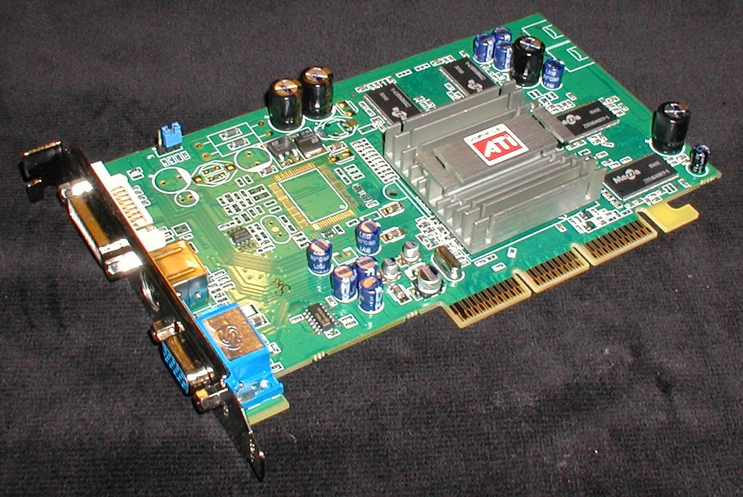 🇨🇦 CanadaRadeon R200
Second-generation ATI GPU with DirectX 8.1 supportGPU · GPU architecture · 2001
 🇺🇸 United StatesKelvin
Nvidia GPU microarchitecture for GeForce 3 and 4 seriesGPU · GPU architecture · 2001
More from Nvidia
All of them WorldGeForce FX series
Nvidia's first DirectX 9 graphics processor lineGPU · GPU architecture · 2003
 WorldGeForce 4 series
Fourth generation of Nvidia GeForce graphics processorsGPU · GPU architecture · 2002
 WorldCurie
Nvidia GPU microarchitecture from 2004 for GeForce 6 and 7 seriesGPU · GPU architecture · 2004
 WorldGeForce 6 series
Sixth generation Nvidia graphics processors with Shader Model 3.0GPU · GPU architecture · 2004