
NetBurst
Intel's Pentium 4-era x86 CPU design, built for very high clock speeds
NetBurst, called P68 inside Intel, was the x86 CPU microarchitecture that succeeded P6. It first shipped in the Willamette-core Pentium 4 on 2000-11-20 and later powered Pentium D, Xeon and Celeron chips. Intel dropped it in 2010 after heat and power problems blocked its planned clock scaling.
- First shipped in the Willamette Pentium 4 on 2000-11-20
- Pipeline grew from 20 stages to 31 in Prescott
- ALUs ran at twice the core clock in the Rapid Execution Engine
- Planned 10 GHz target abandoned; line stopped at 3.8 GHz
- Hyper-threading debuted here in 2002
What it is
NetBurst was the x86 CPU microarchitecture Intel designed as the follow-on to P6. It debuted in the Willamette-core Pentium 4 on 2000-11-20 and went on to underpin every later Pentium 4 and Pentium D, plus the Foster-core Xeon from mid-2001 and Pentium 4-based Celeron parts. Chips ran from 1.3 GHz to 3.8 GHz with one or two cores. The design pushed clock speed hard through a long pipeline and a fast integer unit, and introduced Hyper-threading, an Execution Trace Cache and a replay system. Heat and power limits stopped the planned march to 10 GHz, and Intel retired the line in 2010.
How it came about
Intel built NetBurst to chase ever higher frequencies, aiming for 10 GHz by simply raising the clock over time. The first silicon, Willamette, arrived in November 2000. Northwood followed in January 2002 and Prescott in February 2004. Power and heat ran out of control by November 2004, with the line topping out at 3.8 GHz. Mobile Pentium 4-M fared poorly on performance per watt, so Intel went back to P6, evolving the Tualatin core into Pentium M and then the Core microarchitecture of July 2006. Planned successors Tejas and Jayhawk, with 40 to 50 pipeline stages, were cancelled.
Inside the chip
NetBurst used a very deep instruction pipeline: 20 stages in Willamette and Northwood, 31 in Prescott, against 10 in the Pentium III. Longer pipelines make branch mistakes costly, so Intel added a stronger predictor and the Rapid Execution Engine, where the two arithmetic logic units run at twice the core clock, giving 7.6 GHz effective on a 3.8 GHz chip. An Execution Trace Cache inside L1 holds decoded micro-operations in predicted order. A replay system re-runs operations sent out too early. The front-side bus was quad-pumped, giving 400 MT/s or 800 MT/s effective. Instructions covered x86-16, IA-32 and, on some parts, x86-64, with MMX, SSE, SSE2 and SSE3.
How it was made
NetBurst chips were built across four process generations. Early Willamette steppings used 180 nm with 42M transistors; Northwood moved to 130 nm at 55M. Prescott used 90 nm at 125M, with larger cores at 169M and 230M. Cedar Mill shrank to 65 nm, with counts of 188M, 328M and 376M. Packages spanned Socket 423 and 478 for desktops, Socket 603 and 604 for Xeon, and LGA 771 and LGA 775 later on.
Where it went
The architecture reached desktops through the Pentium 4 and Pentium D, and the budget Celeron and Celeron D lines. Servers and workstations used it from mid-2001, when the Foster core switched Xeon over. Mobile notebooks got the Pentium 4-M, though its heat and poor efficiency made it a weak fit there. Dual-core Pentium D parts paired two Prescott dies in Smithfield, then two Cedar Mill dies in Presler.
Versions and family
Willamette was the first core, replaced by Northwood in January 2002 with more cache, a 130 nm process and Hyper-threading. Prescott arrived in February 2004 on 90 nm with a 31-stage pipeline, 1 MB or 2 MB L2, SSE3 and later EM64T. Cedar Mill was its 65 nm shrink. Dual-core Smithfield put two Prescott cores on one die; Presler used two Cedar Mill dies. The Gallatin core brought L3 cache to the Pentium 4 Extreme Edition. Cancelled successors were Tejas and Jayhawk.
Why it matters
NetBurst pushed retail clock speeds to 3.8 GHz and introduced Hyper-threading, which Intel revived in Nehalem, along with L3 cache on consumer chips. Its trace cache idea returned in simpler form as the Sandy Bridge micro-operation cache. The design also became the cautionary tale behind the megahertz myth: deeper pipelines cut instructions per clock, and rising heat stopped frequency scaling. Intel's roadmap once cast Nehalem as an evolution of NetBurst, but the lineage that shipped ran through Core instead.
Problems and reception
The long pipeline drew criticism because it lowered instructions per clock, and gains from high frequency never offset the loss. Prescott quickly became the hottest and most power-hungry of Intel's single-core x86 and x86-64 chips, capping desktop parts at 3.8 GHz and mobile ones at 3.46 GHz. Shift and rotate operations slowed after the barrel shifter was dropped. Branch prediction hints were allowed in code but dropped on later processors. NetBurst-based production ended on 2008-08-08.
Questions people ask about NetBurst
What is NetBurst?
It is the x86 CPU microarchitecture Intel used in the Pentium 4, Pentium D, Pentium 4-based Celeron and Foster-core Xeon. Known as P68 inside Intel, it replaced P6 and first appeared in the Willamette Pentium 4 on 2000-11-20.
Why did Intel stop using it?
Power and heat blocked the plan to reach 10 GHz. The line stalled at 3.8 GHz in November 2004, and the mobile Pentium 4-M was uncompetitive on performance per watt. Intel returned to P6, leading to Pentium M and then Core in July 2006.
What did the deep pipeline do?
Willamette and Northwood had 20 stages, Prescott 31, versus 10 in the Pentium III. More stages let the chip run faster clocks but raise the cost of a branch misprediction and reduce instructions per clock, so real performance gained less than the frequency suggested.
What is the Execution Trace Cache?
It is a store inside the L1 cache holding decoded micro-operations in their predicted execution order. The CPU can reuse those micro-ops instead of fetching and decoding instructions again, saving time. Sandy Bridge later used a similar but simpler micro-operation cache.
Which sockets did NetBurst chips use?
Desktop and mobile parts used Socket 423, Socket 478 and later LGA 775. Server Xeon parts used Socket 603, Socket 604 and LGA 771.
Good reading and sources
- Checking your browserAnandTech, Article
- Intel cancels Tejas and JayhawkZDNET, Article
- Intel says Adios to Tejas and Jayhawk chipsThe Register, Article
The facts on this page come from the Wikipedia article "NetBurst", written by its contributors and used under the CC BY-SA 4.0 licence, and from its Wikidata record (CC0). EveryChip rewrote the text in its own words, with AI assistance, and compares every page with the article to make sure no passage is copied. It may be reused under the same CC BY-SA 4.0 licence with a link back.
It may contain mistakes, and figures change over time. Nothing here is investment or buying advice. If something is wrong, tell us. Last refreshed 2026-11-14.
Like NetBurst
All CPUs and microprocessors 🇺🇸 United StatesPentium 4
Intel's single-core desktop CPU line built on the NetBurst microarchitectureCPU · x86 · 2000
 🇺🇸 United StatesPentium III
Intel's 32-bit P6 desktop and server CPU line, launched in 1999 with SSE.CPU · x86 · 1999
 🇺🇸 United StatesXeon
Intel's x86 processor brand for servers, workstations and embedded systems since 1998CPU · x86 · 1998
 🇺🇸 United StatesPentium II
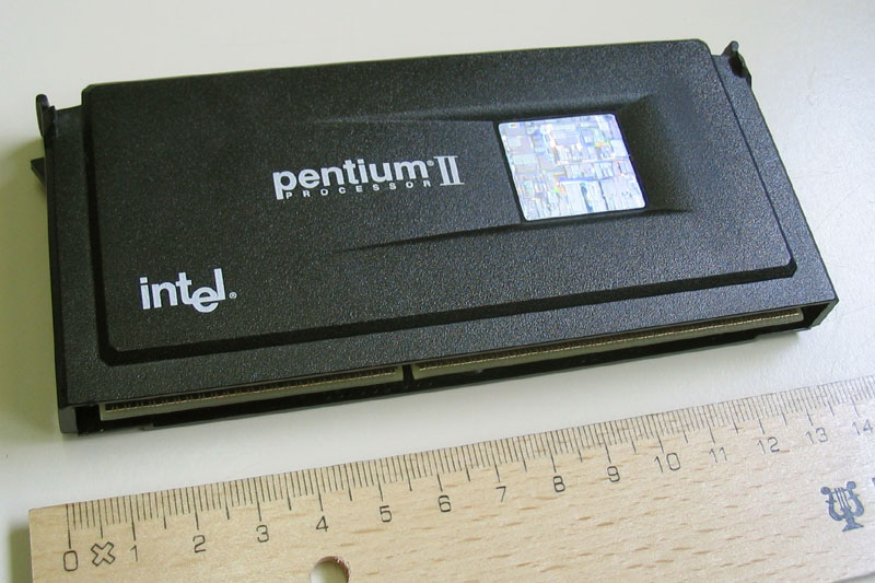
Intel's 1997 P6 desktop CPU line with MMX, sold in a slot cartridgeCPU · x86 · 1997
More from Intel
All of them 🇺🇸 United StatesBlackfin
Hybrid microprocessor and DSP family by Analog DevicesMicrocontroller · RISC · 2000
🇺🇸 United StatesIXP1200
Network processor for mid-range and high-end routersNetwork chip · Arm · 2000
🇮🇱 IsraelTimna
Cancelled Intel CPU with integrated graphics and memory controllerCPU · x86 · 2000
 🇺🇸 United StatesItanium
64-bit EPIC server microprocessor family from Intel and HPCPU · VLIW · 2001