
Intel 8008
Early 8-bit microprocessor from Intel, launched April 1972
The Intel 8008 is an early 8-bit microprocessor introduced in April 1972 and built by Intel on a 10 µm process. Its architecture came from Computer Terminal Corporation for a planned terminal, and it went on to power some of the first commercial personal computers outside calculators.
- Introduced April 1972 with 3,500 transistors
- 8-bit data, 14-bit address, 16 KB memory reach
- Architecture from CTC, silicon built by Intel
- Clocked 500 kHz, up to 800 kHz in the 8008-1
- 18-pin DIP needing about 30 TTL support chips
What it is
The Intel 8008 is an early 8-bit microprocessor that reached the market in April 1972. Intel built it, but the architecture came from Computer Terminal Corporation, which wanted the processor for its Datapoint 2200 terminal. The chip handles 8-bit data and can reach 16 KB of memory through a 14-bit address. It runs at 500 kHz, later 800 kHz in the 8008-1 variant, and packs 3,500 transistors in an 18-pin DIP. Although it began as a part for one customer, an agreement let Intel sell it widely after Seiko asked for it in a calculator. It became a commercial success and led towards the 8080 and the x86 line.
How it came about
CTC designed the architecture to fix heat and other problems in its Datapoint 3300 terminal, moving the CPU onto one chip. Co-founder Austin O. "Gus" Roche took the idea to Intel, where Bob Noyce agreed to a $50,000 contract in early 1970 despite doubts. Texas Instruments joined as a second supplier. Intel engineers Stan Mazor and Ted Hoff proposed a single-chip design, then known as the 1201. TI samples were buggy, and Intel's own work slipped, so CTC shipped the Datapoint 2200 with discrete TTL logic instead. Seiko revived interest in 1971, and Federico Faggin led a redesign to an 18-pin package. CTC later dropped the project, leaving the rights to Intel, which renamed the part 8008 and listed it in April 1972.
Inside the chip
The 8008 uses 8-bit data paths and a 14-bit program counter, with a seven-level call stack. It has one accumulator, A, plus six registers named B, C, D, E, H and L. The H and L pair forms a 14-bit address for memory, giving access to 16 KB. There are 48 instructions, from one to three bytes long, covering loads, arithmetic, logic, jumps, calls and returns. Four flag bits record carry, parity, zero and sign. Everything runs on 8 bits only, with no 16-bit operations. Because the 18-pin package is small, one 8-bit bus carries data, addresses and status in turn, and about 30 TTL support chips are needed around it.
How it was made
Intel built the 8008 with 10 µm silicon-gate enhancement-mode PMOS logic, holding 3,500 transistors. Early parts ran up to 0.5 MHz, and the 8008-1 raised the specified maximum to 0.8 MHz. Instructions take 3 to 11 T-states, each T-state being two clock cycles. The chip ships in an 18-pin dual in-line package, which limits the pins available and forces the shared bus design. Texas Instruments also produced samples from Intel drawings, under the name TMX 1795, but those were rejected as buggy.
Where it went
The 8008 was meant for CTC's Datapoint 2200 terminal, and Seiko wanted it for a calculator. It went on to serve computer terminals, calculators, bottling machines, ASEA industrial robots such as the IRB 6, and simple computers. It powered the SCELBI kit, the French Micral N and the Canadian MCM/70, the first commercial personal computers outside the calculator world. Hewlett-Packard used it in early models of its 2640 terminal family. In the UK, a team at S. E. Laboratories Engineering built a microcomputer around a pre-release sample in 1972.
Versions and family
The 8008-1 is a faster version rated to 0.8 MHz. The chip followed the Intel 4004 in the catalogue, though it is not based on that design. Its successor, the Intel 8080, moved to a 40-pin NMOS package, widened the bus and grew the registers and instruction set, but it is not binary compatible. The 8085 modernised the 8080 electrically, and the 8086 extended the 8080, so traces of the original design persist in x86.
Why it matters
The 8008 sold well and helped prove that a single-chip CPU could be a product in its own right. It powered some of the earliest commercial personal computers and many terminals and control systems. Its instruction set shaped later chips: most Datapoint 2200 and 8008 instructions have counterparts in the 8080, 8085, Z80 and modern x86, though the encodings differ. Gary Kildall wrote the PL/M language for it, the first language aimed at a microprocessor, and later an 8008 simulator called INTERP/8.
Problems and reception
Bob Noyce was doubtful at first, arguing that a processor sells one chip per computer while memory sells many, and that selling a CPU might drive memory customers away. TI's TMX 1795 samples were buggy and were rejected. The 8008 is slower in instructions per second than the 4-bit 4004 and 4040, yet its 8-bit data handling and larger memory reach gave it the edge in most uses. Interrupt support is only partial, since the chip cannot save its own state without outside help.


Questions people ask about Intel 8008
Who designed the Intel 8008?
Computer Terminal Corporation created the architecture, with Victor Poor and Harry Pyle on the instruction set. Intel handled the silicon. Ted Hoff and Stan Mazor proposed the single-chip approach, Federico Faggin led the project from 1971, and Hal Feeney did the detailed logic and layout.
How much memory could it use?
The 8008 addresses 16 KB of memory. The H and L registers join to form a 14-bit address, and each memory cell holds 8 bits. The upper two address bits are ignored, and the chip can reach 8 input ports and 24 output ports.
Was it related to the Intel 4004?
Intel named it 8008 to suggest a step from the 4004, but the two are not related in design. The 8008 work actually began before the 4004. It is an 8-bit part, while the 4004 and 4040 are 4-bit, and the 8008 handles more memory.
What came after it?
The Intel 8080 succeeded it, using a 40-pin NMOS package and a better external bus. The two are not binary compatible, though assemblers could translate source code. The 8085 followed the 8080, and the 8086 extended that line into x86.
Good reading and sources
The facts on this page come from the Wikipedia article "Intel 8008", written by its contributors and used under the CC BY-SA 4.0 licence, and from its Wikidata record (CC0). EveryChip rewrote the text in its own words, with AI assistance, and compares every page with the article to make sure no passage is copied. It may be reused under the same CC BY-SA 4.0 licence with a link back.
It may contain mistakes, and figures change over time. Nothing here is investment or buying advice. If something is wrong, tell us. Last refreshed 2026-11-14.
Like Intel 8008
All CPUs and microprocessors 🇯🇵 JapanHitachi 6309
Hitachi's CMOS 8-bit microprocessor, a faster and richer 6809CPU · 8-bit · 1985
 🇯🇵 JapanHD64180
A Z80-based embedded microprocessor with on-chip MMU and peripheralsCPU · 8-bit · 1985
 WorldMOS Technology 6510
8-bit 6502-derived CPU with a built-in I/O port, used in the Commodore 64CPU · 8-bit
🇺🇸 United StatesRockwell PPS-8
An early 8-bit microprocessor from Rockwell with unusual code-saving featuresCPU · 8-bit · 1974
More from Intel
All of them 🇺🇸 United StatesIntel 4004
The first commercial microprocessor, a 4-bit chip released by Intel in 1971.CPU · Other · 1971
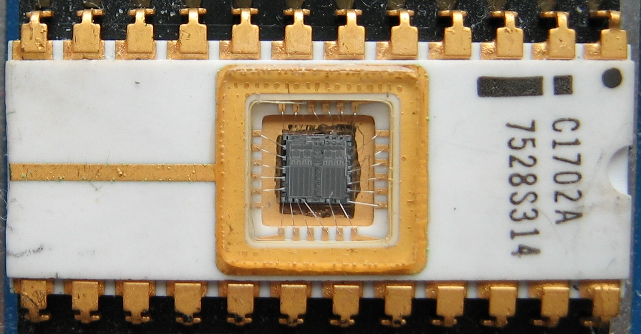 🇺🇸 United StatesEPROM
Non-volatile memory chip erased by ultraviolet lightMemory · 1971
 🇺🇸 United StatesUART
Chip for serial data communication between devicesAnalog · 1971
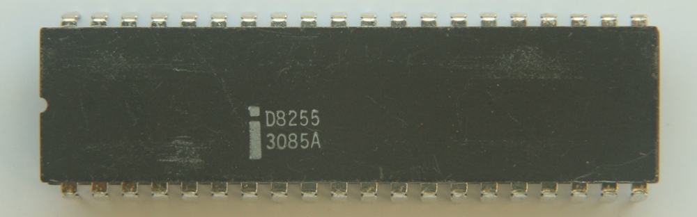 🇺🇸 United StatesIntel 8255
Programmable parallel input/output interface chip for early microprocessorsAnalog · 1970