
Skylake
Intel's 2015 sixth-generation Core microarchitecture, built on 14 nm
Skylake is the codename for Intel's sixth-generation Core microprocessor family, launched on 5 August 2015 as a redesign on the same 14 nm process as Broadwell. Developed mainly by Intel Israel in Haifa, it spanned chips from 4.5 W tablets to 28-core servers and became the base for Kaby Lake, Coffee Lake, Whiskey Lake and Comet Lake.
- Launched 5 August 2015 as Intel's sixth-generation Core family
- 14 nm process, a tock redesign over Haswell and Broadwell
- 2 to 28 cores, clock speeds up to 5.0 GHz
- First Intel client cores with SGX and MPX; AVX-512 on Xeon and X-series
- Gen9 GPU with up to 72 execution units and HEVC encode/decode
What it is
Skylake is the codename for Intel's sixth generation of Core microprocessors, a family covering desktops, laptops, tablets, workstations and servers. It arrived on 5 August 2015 and replaced both Haswell and Broadwell. The design kept the 14 nm process but reworked the CPU and GPU, so it counted as a "tock" in Intel's tick-tock cycle of alternating new processes and new designs. Intel claimed higher CPU and GPU performance with lower power draw. Chips spanned 2 to 28 cores and clock speeds up to 5.0 GHz, sold under Core i3, i5, i7, i9, Core m, Xeon, Pentium and Celeron names.
How it came about
Most of the work was done by Intel Israel at its Haifa research centre, following earlier projects such as Banias, Dothan, Conroe and Sandy Bridge. The team evolved Haswell's design, adding small performance gains and power-saving features, with a key goal of scaling down to 4.5 W for tablets and notebooks. Intel revealed Skylake at its Developer Forum in San Francisco in September 2014, showing a desktop testbed and a laptop playing 4K video. The i5-6600K and i7-6700K went on sale at Gamescom on 5 August 2015, soon after Broadwell, whose 14 nm delays had pushed its own launch back.
Inside the chip
The CPU gained a stronger front end, deeper out-of-order buffers, a third vector integer ALU giving five arithmetic units, wider load/store paths and better hyper-threading. The re-order buffer grew to 224 entries and L2 cache became 4-way set associative. Cache per core is 32 KB instructions plus 32 KB data in L1, 256 KB in L2 (1 MB on Skylake-X, SP and W), with up to 38.5 MB shared L3 and 128 MB of eDRAM L4 on Iris Pro parts. New instructions include MPX memory protection and SGX secure enclaves; Xeon parts add AVX-512. The Gen9 GPU reaches 72 execution units and handles DirectX 12_1, OpenGL 4.6 and HEVC encode and decode.
How it was made
Intel built Skylake on its 14 nm bulk silicon process with Tri-Gate (FinFET) transistors, the same node as Broadwell. Production was in-house at Intel fabs. Packaging split by market: LGA 1151 for mainstream desktops, LGA 2066 for X-series enthusiasts, LGA 3647 for servers, and several BGA options for mobile parts. The fully integrated voltage regulator used on Haswell was moved back to the motherboard, and the link to the platform controller hub was upgraded to DMI 3.0 at up to 8 GT/s.
Where it went
Skylake chips went into desktops, gaming PCs, laptops, tablets, workstations and servers, appearing across the Core i3 to i9 ranges, Core m, Xeon E3 and Xeon Scalable lines. They paired with Intel 100-series (Sunrise Point) and 200-series chipsets, plus X299 for X-series. The platform supported DDR3L and DDR4 memory, Thunderbolt 3, SATA Express, NVMe over PCIe 3.0 x4, and up to three displays via HDMI 1.4, DisplayPort 1.2 or eDP. VGA output was dropped. Skylake is the last Intel platform officially supported by Windows versions older than Windows 10.
Versions and family
Five variants were produced, marked S, X, H, U and Y. S and X use LGA sockets and include unlocked K and X models; H, U and Y are BGA parts for mobile. P models cut the GPU to 12 execution units instead of 24. Skylake-X, SP and W carry larger 1 MB L2 per core and AVX-512. The design was reused in Kaby Lake, Coffee Lake, Whiskey Lake and Comet Lake. Successors include Kaby Lake for mainstream systems, Cascade Lake for high-end servers and workstations, and Palm Cove on the process side.
Why it matters
Skylake shortened Broadwell's run and set the template for several later Intel generations that shared its core design. It brought AVX-512, SGX and MPX into the product line and pushed integrated graphics to 72 execution units with strong media acceleration. Its wide spread, from 4.5 W tablets to 28-core server parts, made it one of Intel's broadest families. Desktop LGA 1151 chips were discontinued on 4 March 2019, apart from the i3-6100, i5-6500 and Xeon E3 v5.
Problems and reception
Non-K chips could be overclocked by raising the base clock through beta UEFI updates, a route ASRock promoted as Sky OC, but it broke C-states, turbo boost, integrated graphics and temperature readings and slowed AVX2. Intel blocked it with microcode in February 2016. Microsoft's plan to cut Windows 7 and 8.1 support drew criticism and was later softened. Skylake is vulnerable to Spectre, more so than some peers because of extra indirect branch speculation, and a microcode fix addressed erratic behaviour in short instruction loops with hyper-threading.


Questions people ask about Skylake
What exactly is Skylake?
Skylake is the codename for Intel's sixth-generation Core microprocessor design. It is a CPU microarchitecture, not a single chip, and it appeared in many products from low-power Core m parts to Xeon server processors between 2015 and 2019.
Who designed it and where?
Intel designed it, with the main work carried out by Intel Israel at its engineering research centre in Haifa. That team had earlier produced designs such as Banias, Dothan, Conroe and Sandy Bridge.
What process was it built on?
Intel manufactured Skylake on its own 14 nm process using Tri-Gate (FinFET) transistors. That was the same node as Broadwell, so Skylake counted as a design step rather than a shrink in Intel's tick-tock model.
What memory does it take?
Mainstream parts work with both DDR3L and DDR4 SDRAM, reflecting the market's shift between the two standards at the time. LGA 1151 systems support up to 64 GB, and a UniDIMM SO-DIMM type was introduced to carry either memory type.
Which operating systems do Skylake machines support?
Windows 10 is the main supported Microsoft OS. Microsoft initially planned to end Windows 7 and 8.1 support in 2017 but later extended full support to the end of those products' lifecycles. Linux support arrived over kernel versions 4.10 and 4.11, and OpenBSD 6.2 supports it fully.
Good reading and sources
- Checking your browserAnandTech, Article
- Intel® ProcessorsIntel, Article
- Intel Skylake CPU details revealed: These faster, more power-efficient chips can even drive three 4K monitorsPCWorld, Article
The facts on this page come from the Wikipedia article "Skylake (microarchitecture)", written by its contributors and used under the CC BY-SA 4.0 licence, and from its Wikidata record (CC0). EveryChip rewrote the text in its own words, with AI assistance, and compares every page with the article to make sure no passage is copied. It may be reused under the same CC BY-SA 4.0 licence with a link back.
It may contain mistakes, and figures change over time. Nothing here is investment or buying advice. If something is wrong, tell us. Last refreshed 2026-11-14.
Like Skylake
All CPUs and microprocessors 🇺🇸 United StatesBroadwell
Intel's 14 nm shrink of the Haswell CPU microarchitectureCPU · x86 · 2014
 🇺🇸 United StatesHaswell
Intel's 2013 x86-64 CPU microarchitecture on 22 nm FinFETCPU · x86 · 2013
 🇺🇸 United StatesIvy Bridge
Intel's 22 nm tick microarchitecture featuring FinFET transistors and integrated graphics.CPU · x86 · 2012
 🇮🇱 IsraelIce Lake
Intel 10 nm mobile and server processors with Sunny Cove coresCPU · x86 · 2019
More from Intel
All of them 🇺🇸 United StatesXeon D
Intel's low-power x86 system-on-chip line for microserversCPU · x86 · 2015
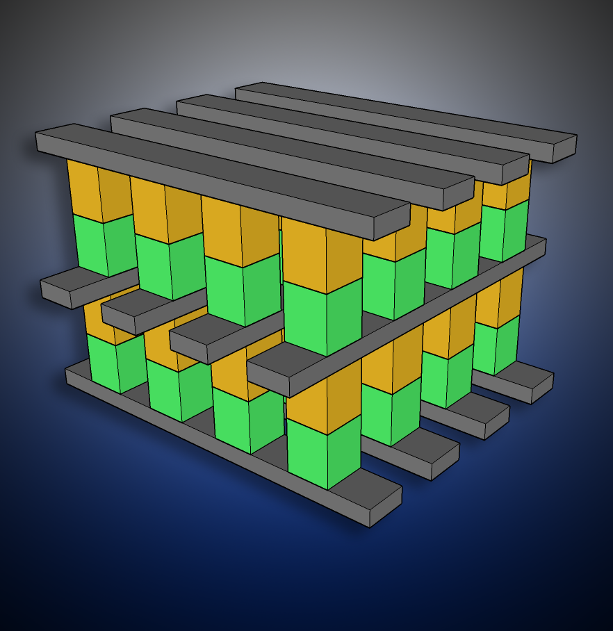 🇺🇸 United States3D XPoint
Non-volatile memory from Intel and Micron, sold as OptaneMemory · 2015
 🇺🇸 United States and 1 moreKaby Lake
Intel's 7th-gen Core CPUs on a refined 14 nm processCPU · x86 · 2016
🇺🇸 United States and 1 moreGoldmont
Low-power Atom microarchitecture for entry-level SoCs, up to four cores.CPU · x86 · 2016