
Haswell
Intel's 2013 x86-64 CPU microarchitecture on 22 nm FinFET
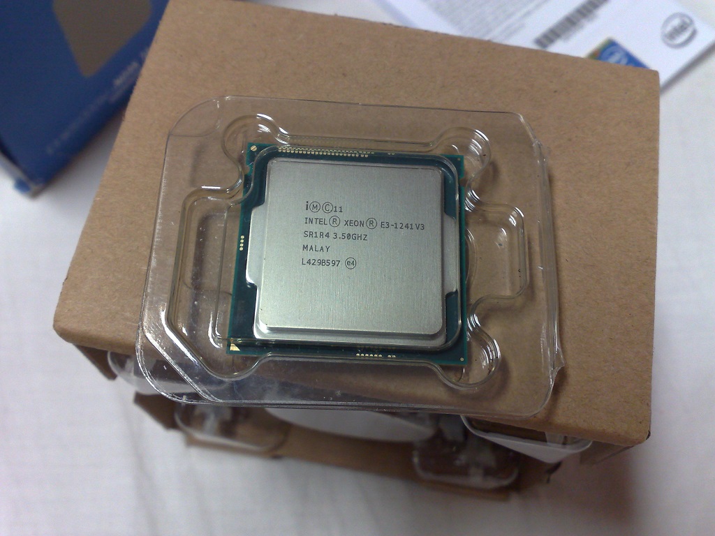
Haswell is a CPU microarchitecture from Intel, first released on 4 June 2013 as the tock step of the Tick–tock model. It kept the 22 nm FinFET process of Ivy Bridge but widened the cores, added AVX2 and FMA3, and moved the voltage regulator onto the die, powering Core, Xeon v3, Pentium and Celeron chips.
- Released 4 June 2013 as Intel's tock step on 22 nm FinFET
- First Intel cores with AVX2 and FMA3, plus a 192-entry out-of-order window
- GT3e graphics pair 40 execution units with 128 MB of on-package eDRAM
- Desktop die: 1.4 billion transistors, 177 mm2; server die: 5.56 billion, 661 mm2
- TSX was switched off by microcode in August 2014 after a bug was found
What it is
Haswell is a microarchitecture for x86-64 central processing units, designed and made by Intel. It reached the market on 4 June 2013, announced at Computex Taipei that day after an early showing at the 2011 Intel Developer Forum. In Intel's Tick–tock schedule it is a tock: a new design built on the same 22 nm FinFET process as Ivy Bridge before it. Chips based on it were sold as 4th generation Core, Xeon E3/E5/E7 v3, plus Pentium and Celeron models. Notable points include wider cores, AVX2 and FMA3 instructions, a voltage regulator built into the package, and integrated graphics up to Iris Pro 5200 with 128 MB of eDRAM.
How it came about
Intel first demonstrated Haswell silicon at its Developer Forum in 2011. The formal announcement came on 4 June 2013 at Computex Taipei. Chips went to PC makers and OEMs in the middle of 2013, and separate desktop parts reached retail in September that year. A mid-2014 refresh, simply called Haswell Refresh, raised clock speeds by about 100 MHz and arrived alongside the 9 Series chipsets. The K-series refresh parts were codenamed Devil's Canyon. At least one Haswell part, the Pentium G3420, was still on sale in 2022.
Inside the chip
Each core gained a fourth arithmetic logic unit, a third address generation unit and a second branch execution unit, with deeper buffers and more cache bandwidth. The out-of-order window grew from 168 to 192 entries. A micro-operation cache holds about 1.5 K micro-ops, and the pipeline runs 14 to 19 stages depending on whether it hits. New instructions include AVX2, FMA3, BMI1, BMI2 and gather. The integrated GPU comes in GT1, GT2, GT3 and GT3e forms; GT3 has 40 execution units against Ivy Bridge's 16, and GT3e adds 128 MB of eDRAM, called Crystalwell, acting as a shared level 4 cache.
How it was made
Haswell reused the 22 nm Tri-Gate FinFET process from Ivy Bridge. Desktop parts carry 1.4 billion transistors on a 177 mm2 die, while server parts reach 5.56 billion transistors over 661 mm2. Intel fabricated the chips itself. Packages include LGA 1150 for mainstream desktops, LGA 2011-v3 for enthusiast and server parts, rPGA 947 and BGA 1364/1168 for mobile. The platform controller hub shrank from 65 nm to 32 nm.
Where it went
Desktop chips sat in LGA 1150 boards with Intel 8 and 9 Series chipsets, and in LGA 2011-v3 boards with the X99 chipset. Mobile versions went into laptops and Ultrabooks, with ULT and ULX parts at 13.5 W, 15 W and 10 W for thin designs and tablets. Haswell-H served all-in-one PCs and small boards. Server parts arrived as Xeon E3 v3, then E5 v3 in September 2014 and E7 v3 in May 2015. Windows 7 through Windows 10 were released for the design.
Versions and family
The family splits into Haswell-DT for desktops, Haswell-MB for laptops, Haswell-H, ULT and ULX for small and low-power systems, and Haswell-E, EP and EX for enthusiasts and servers. ULT and ULX are dual-core only. Refresh parts added roughly 100 MHz, and Devil's Canyon K-series parts improved the thermal interface material, raised TDP to 88 W and added VT-d. Ivy Bridge came before it; Broadwell shrank the process and Skylake replaced the architecture.
Why it matters
Haswell widened Intel cores and brought 256-bit AVX2 into mainstream PCs, and its eDRAM package showed a way to feed a strong integrated GPU. The design reached from 10 W tablets to 18-core Xeons, and one Pentium part was still sold in 2022. Its low-power C6 and C7 states pushed PC makers to rework power supplies.
Problems and reception
Compared with Ivy Bridge, Haswell was measured at about 3% better overall, with up to 5% more single-thread and 6% more multi-thread performance, and up to 20% faster integrated graphics. Desktop parts drew 8% to 23% more power under load and ran about 15 °C hotter, though clocks above 4.6 GHz were achievable. In August 2014 Intel found a bug in Transactional Synchronization Extensions and disabled TSX by microcode on most parts, leaving it working only on Haswell-EX.


Questions people ask about Haswell
What kind of chip is Haswell?
Haswell is not one chip but a CPU microarchitecture from Intel. Many products were built on it, from Core i3/i5/i7 desktop and laptop parts to Xeon E3, E5 and E7 v3 server processors, plus Pentium and Celeron models.
What did Haswell change over Ivy Bridge?
It kept the 22 nm FinFET process but widened each core with an extra arithmetic logic unit and address unit, enlarged buffers, added AVX2 and FMA3 instructions, and put the voltage regulator on the package. Integrated graphics gained execution units and optional eDRAM.
Why was TSX turned off?
Intel announced in August 2014 that a bug existed in the Transactional Synchronization Extensions implementation on Haswell, Haswell-E, Haswell-EP and early Broadwell steppings. A microcode update disabled the feature on those parts. Haswell-EX kept working TSX.
What is Crystalwell?
Crystalwell is the 128 MB of embedded DRAM placed on the package with GT3e graphics, found in Iris Pro 5200 models. It acts as a level 4 cache, shared on demand between the CPU and GPU and serving as a victim cache for the level 3 cache.
Which sockets did Haswell use?
Mainstream desktops used LGA 1150, enthusiast and server parts used LGA 2011-v3, laptops used rPGA 947, and BGA 1364 and BGA 1168 covered soldered mobile and small-form-factor designs.
Good reading and sources
- Checking your browserAnandTech, Article
- Data CenterIntel, Article
- Intel’s power-efficient Haswell processor targets thinner laptops with new 10-watt TDPThe Verge, Article
- Haswell (microarchitecture) on WikipediaEncyclopedia
- More photos on Wikimedia CommonsPhotos
- Wikidata recordOpen data
The facts on this page come from the Wikipedia article "Haswell (microarchitecture)", written by its contributors and used under the CC BY-SA 4.0 licence, and from its Wikidata record (CC0). EveryChip rewrote the text in its own words, with AI assistance, and compares every page with the article to make sure no passage is copied. It may be reused under the same CC BY-SA 4.0 licence with a link back.
It may contain mistakes, and figures change over time. Nothing here is investment or buying advice. If something is wrong, tell us. Last refreshed 2026-11-14.
Like Haswell
All CPUs and microprocessors 🇺🇸 United StatesIvy Bridge
Intel's 22 nm tick microarchitecture featuring FinFET transistors and integrated graphics.CPU · x86 · 2012
 🇺🇸 United StatesBroadwell
Intel's 14 nm shrink of the Haswell CPU microarchitectureCPU · x86 · 2014
 🇺🇸 United States and 1 moreSkylake
Intel's 2015 sixth-generation Core microarchitecture, built on 14 nmCPU · x86 · 2015
 🇺🇸 United StatesYonah
Intel's first 65 nm mobile CPU cores, sold as Core Duo and Core SoloCPU · x86 · 2006
More from Intel
All of them 🇺🇸 United StatesIntel Quark
Low-power 32-bit x86 system on a chip for wearables and IoT.SoC · x86 · 2013
 🇺🇸 United StatesSilvermont
Intel's 22 nm low-power Atom core design, used across four SoC familiesCPU · x86 · 2013
🇺🇸 United StatesIntel XMM modems
Intel's series of 4G and 5G cellular modems for phones, tablets and laptopsModem · 2013
🇺🇸 United StatesAtom
Low-power x86 system on a chip for mobile and embedded devices.SoC · x86 · 2012