
PC133
Standard for 133 MHz synchronous dynamic RAM modules
PC133 is a memory module standard for SDR SDRAM chips operating at 133 MHz. It followed the PC100 specification to ensure reliable high-speed performance in computers. The format uses synchronous timing coordinated by an external clock signal.
- Operates at 133 MHz clock frequency
- Follows Intel PC100 reliability guidelines
- Uses synchronous interface with external clock
- Part of single data rate SDRAM family
- Supports pipelined commands for efficiency
What it is
PC133 refers to a specific class of synchronous dynamic random-access memory modules. These components operate at a clock frequency of 133 megahertz. The designation ensures that the memory meets strict timing requirements for stable operation. It belongs to the single data rate SDRAM family, which coordinates data transfer with an external clock signal. This standard helped unify performance expectations for personal computer memory during the late 1990s and early 2000s.
How it came about
The development of PC133 followed the introduction of the PC100 standard by Intel. Early 100 MHz modules sometimes failed to operate reliably at their rated speed. Intel published guidelines to define robust manufacturing requirements for 100 MHz operation. As system speeds increased, the industry adopted the PC133 label for modules capable of running at 133 MHz. This progression allowed computers to achieve higher data bandwidth without changing the fundamental memory architecture.
Inside the chip
SDRAM divides internal storage into independent banks that can operate simultaneously. This structure allows the chip to process commands in different sections at the same time. Pipelining enables the memory to accept new instructions before finishing previous tasks. Control signals such as row and column address strobes select specific commands. The clock enable line manages when the chip processes inputs, while data mask lines suppress input or output as needed.
How it was made
Manufacturers produce these chips using complementary metal-oxide-semiconductor fabrication processes. The first commercial SDRAM appeared in 1992 from Samsung Electronics. By 2000, synchronous memory had replaced asynchronous types in most computers due to better performance. Major producers include Samsung, SK Hynix, Micron Technology, ChangXin Memory Technologies, and Nanya Technology. They build modules containing multiple chips to create wider data paths for systems.
Where it went
PC133 modules were widely used in desktop computers and workstations requiring faster memory access. Servers also utilized registered varieties of this memory for greater scalability. The standard facilitated interoperability between components from different manufacturers. Systems could interleave operations across memory banks to increase effective bandwidth. This approach improved overall system responsiveness compared to older asynchronous memory designs.
Versions and family
The PC133 standard sits between PC100 and later double data rate specifications. DDR SDRAM was demonstrated in 1997 and released commercially in 1998. Subsequent generations like DDR2 and DDR3 introduced wider mode registers and new commands. PC133 remains part of the single data rate lineage, distinct from the double data rate families that followed. JEDEC maintains the open standards that govern these various memory types.
Why it matters
This standard helped establish consistent naming conventions for memory speed. The PC prefix became a common identifier for module performance levels. It ensured that consumers and engineers could identify compatible components easily. The shift to synchronous operation marked a significant change in how memory interacted with processors. Higher clock multiples allowed bandwidth to increase even as basic latency times remained similar.


Questions people ask about PC133
What does PC133 mean?
PC133 identifies synchronous dynamic RAM modules that operate reliably at 133 MHz. It follows the naming convention established by Intel for PC100 memory. The number indicates the clock speed the module supports.
How does SDRAM differ from older DRAM?
SDRAM uses an external clock signal to coordinate operations. Older asynchronous DRAM responded directly to control signals without a clock. Synchronous design allows for pipelining and higher data transfer rates through interleaved bank access.
Who sets the standards for this memory?
JEDEC, an electronics industry association, adopts open standards for SDRAM. They formalized the first SDRAM standard in 1993. Intel also published specific guidelines for PC100 and PC133 module reliability.
Good reading and sources
The facts on this page come from the Wikipedia article "Synchronous dynamic random-access memory", written by its contributors and used under the CC BY-SA 4.0 licence, and from its Wikidata record (CC0). EveryChip rewrote the text in its own words, with AI assistance, and compares every page with the article to make sure no passage is copied. It may be reused under the same CC BY-SA 4.0 licence with a link back.
It may contain mistakes, and figures change over time. Nothing here is investment or buying advice. If something is wrong, tell us. Last refreshed 2026-11-14.
Like PC133
All memory chips WorldDRAM
Volatile semiconductor memory using capacitors and transistors for high-density storage.Memory
 🇺🇸 United StatesPC100
Intel standard for reliable 100 MHz SDRAM modulesMemory
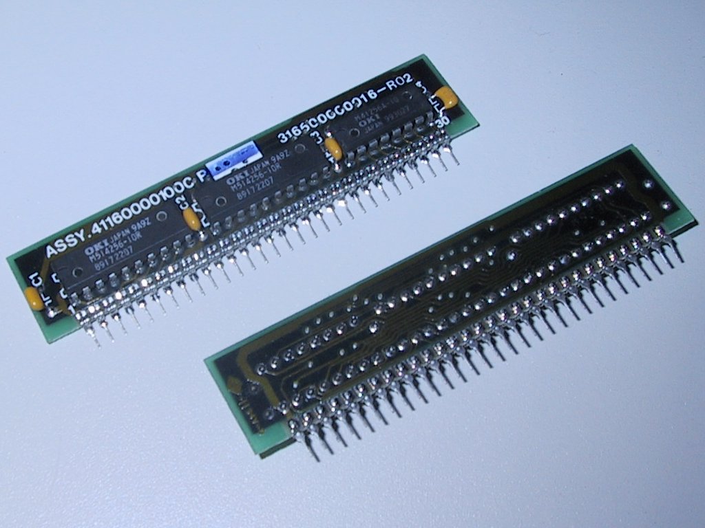 WorldSIPP memory
Pin-based 30-pin memory module for early PCsMemory
More from Intel
All of them WorldIntel 8279
Programmable keyboard and display controller for Intel microprocessorsAnalog
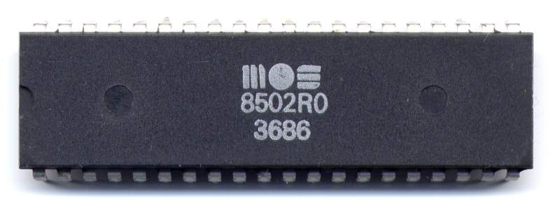 WorldMOS Technology 8502
An 8-bit CPU from MOS Technology that powered the Commodore 128CPU · 8-bit
 🇺🇸 United StatesRapidCAD
A 486DX in a 386 socket, with a dummy FPU chip to match.CPU · x86
🇺🇸 United StatesTolapai
Intel embedded SoC with Pentium M core and security accelerationSoC · x86