Tolapai
Intel embedded SoC with Pentium M core and security acceleration
Tolapai is an embedded system on a chip from Intel that integrates a Pentium M processor, memory controllers and security hardware. It marked Intel's first single-chip x86 solution combining processor and chipset since the mid-1990s.
- First Intel x86 SoC with integrated chipset since 1994
- Combines Pentium M core with QuickAssist security unit
- Features 148 million transistors on 90 nm process
- Includes three Gigabit Ethernet MACs and PCIe support
What it is
Tolapai is an embedded system on a chip developed by Intel. It combines a Pentium M processor core based on the Dothan microarchitecture with DDR2 memory controllers and input/output interfaces. The chip also includes a QuickAssist accelerator unit designed for security functions. This integration allows it to handle processing, memory management and peripheral connections on a single piece of silicon. It represents a significant consolidation of components typically found on separate chips in embedded systems.
How it came about
This processor was Intel's first integrated x86 solution to combine the processor, chipset and memory controller on one die since the 80386EX in 1994. By merging these elements, Intel aimed to simplify design for embedded applications. The project brought together computing power with dedicated security acceleration, addressing the needs of networked devices that require both performance and data protection in a compact form factor.
Inside the chip
The chip uses a single Pentium M core running between 600 MHz and 1.2 GHz. It features 256 KB of cache and supports MMX, SSE, SSE2, SSE3 and XD bit instructions. Memory support includes DDR2 speeds from 400 to 800 MHz, with options for error correction. Connectivity is extensive, featuring three Gigabit Ethernet media access controllers, PCI Express lanes, SATA storage interfaces and USB ports. It also includes serial ports, CAN bus interfaces and general purpose input/output pins for industrial control tasks.
How it was made
Manufactured using 90 nanometre process technology, the die contains 148 million transistors and measures 225 square millimetres. It is housed in a 1088-ball flip chip ball grid array package with a pitch of 1.092 mm. The total package size is 37.5 mm by 37.5 mm. Intel produced the chip, which operates at temperatures from 0 to 70 degrees Celsius for most models, with some rated for -40 to 85 degrees Celsius.
Where it went
Tolapai targets embedded computing environments where space and integration are critical. Its built-in networking interfaces and security acceleration make it suitable for network appliances, such as firewalls and virtual private network gateways. The inclusion of industrial interfaces like CAN bus and multiple serial ports allows it to serve in automation and control systems. It consolidates what would otherwise require multiple discrete components into a single board solution.
Versions and family
The product line is identified as the Intel EP80579 integrated processor. All models share the same instruction set support and basic architecture. Variations exist primarily in operating temperature ranges, with standard commercial versions and extended industrial grade options available. The stepping identified for this silicon is B1.
Why it matters
By reintegrating the memory controller and chipset with the x86 core, Tolapai demonstrated a shift towards higher integration in embedded markets. It paved the way for subsequent low-power system on a chip designs from Intel, such as the Atom and Quark families. The inclusion of hardware security acceleration highlighted the growing importance of cryptographic operations in embedded network devices.
Questions people ask about Tolapai
What processor core does Tolapai use?
It uses a single Pentium M core based on the Dothan microarchitecture. The clock speed ranges from 600 MHz to 1.2 GHz, and it supports legacy x86 instruction sets including SSE3.
What makes Tolapai different from standard desktop CPUs?
It is a system on a chip that integrates the memory controller, input/output interfaces and security acceleration directly onto the processor die. This reduces the need for external chipset components in embedded designs.
What kind of memory does it support?
The chip supports DDR2 memory with speeds ranging from 400 MHz to 800 MHz. It can interface with dual in-line memory modules or soldered memory, with optional error correction code support.
Good reading and sources
The facts on this page come from the Wikipedia article "Tolapai", written by its contributors and used under the CC BY-SA 4.0 licence, and from its Wikidata record (CC0). EveryChip rewrote the text in its own words, with AI assistance, and compares every page with the article to make sure no passage is copied. It may be reused under the same CC BY-SA 4.0 licence with a link back.
It may contain mistakes, and figures change over time. Nothing here is investment or buying advice. If something is wrong, tell us. Last refreshed 2026-11-14.
Like Tolapai
All systems on a chip 🇺🇸 United StatesXeon D
Intel's low-power x86 system-on-chip line for microserversCPU · x86 · 2015
 🇺🇸 United StatesXScale
ARM-based microarchitecture for mobile and embedded systemsCPU · Arm · 2002
 🇺🇸 United StatesIntel Atom
Intel's low-power x86 processor line for netbooks, embedded and server useCPU · x86 · 2008
🇺🇸 United StatesBonnell
Intel's low-power x86 microarchitecture behind early Atom chipsCPU · x86 · 2008
More from Intel
All of them WorldIntel 8279
Programmable keyboard and display controller for Intel microprocessorsAnalog
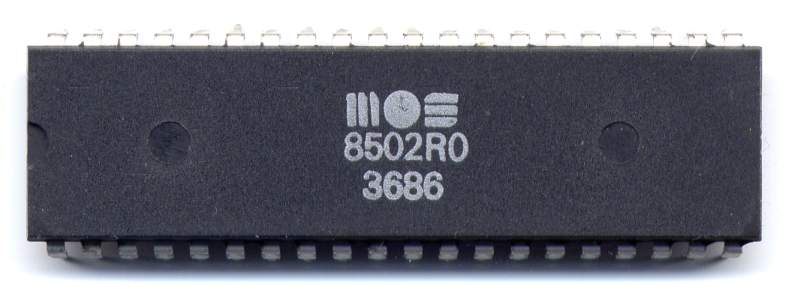 WorldMOS Technology 8502
An 8-bit CPU from MOS Technology that powered the Commodore 128CPU · 8-bit
 🇺🇸 United StatesRapidCAD
A 486DX in a 386 socket, with a dummy FPU chip to match.CPU · x86
 🇺🇸 United States and 1 moreMCS-96
A 16-bit microcontroller family for embedded control systems.Microcontroller · Other