
Intel 486DX2
A 486 CPU whose internal clock ran at twice the bus speed
The Intel 486DX2 is a central processing unit that Intel launched in 1992. It took the existing 486DX design and added a clock multiplier, so the core ran at double the rate of the external bus. That gave a speed gain without demanding a faster motherboard bus, and it shipped in 25/50 MHz and 33/66 MHz forms.
- Internal clock ran at double the external bus rate
- Sold as 25/50 MHz and 33/66 MHz parts on an 800 nm process
- P24D revision added write-back caching to the L1 cache
- 3.3 V variant drew 1.5 W, under 60% of the 5 V part
- Dhrystone V1.1: 40 MIPS at 50 MHz, 54 MIPS at 66 MHz
What it is
The Intel 486DX2 is a desktop and embedded central processing unit that Intel brought out in 1992. It belongs to the 486 generation and speaks the x86-16 and IA-32 instruction sets. Its defining trick is a clock multiplier: the chip's inner logic runs at twice the frequency of the bus it talks to. Two speed grades were sold, pairing a 25 MHz bus with a 50 MHz core and a 33 MHz bus with a 66 MHz core. Both were built on an 800 nm process. The part is now unsupported.
How it came about
Intel based the DX2 on the earlier 486DX, adding the multiplier so that instruction throughput could rise without any change to the board-level bus. Two production revisions appeared, coded P24 and P24D. The second of these brought a quicker L1 cache mode. AMD and Cyrix later sold rival chips aimed at the same slot. A low-voltage 50 MHz variant with System Management Mode was planned for the closing quarter of 1994.
Inside the chip
Inside, the DX2 keeps the 486DX core but clocks it at double the rate seen by the outside bus, so a 33 MHz board can host a 66 MHz processor. The first revision, P24, could only run its level-one cache in write-through mode, where every store goes straight to main memory. P24D added write-back, holding changed data in the cache until it is needed elsewhere, which speeds things up. The instruction set covers x86-16 and IA-32.
How it was made
Both speed grades were fabricated on an 800 nm process at Intel. A later 3.3 volt, 50 MHz variant drew 1.5 watts, under 60 percent of what the 5 volt part consumed. That chip sat in a 208-lead small quad flat package, a surface-mount case that saved 30 percent of the board space and 40 percent of the volume taken by the plastic quad flat package on the standard Intel486.
Where it went
The DX2 went into personal computers built around the 486 platform, where it offered more speed without a redesign of the motherboard bus. Intel also published datasheets and promoted an embedded version of the i486DX2, pointing the part at industrial and dedicated systems as well as desktops.
Versions and family
Two main steppings exist. P24 is the original, limited to write-through caching, while P24D supports the faster write-back mode. Speed pairs were 25/50 MHz and 33/66 MHz. Intel later readied a 3.3 volt 50 MHz model with System Management Mode in a 208-lead SQFP. AMD and Cyrix made competing equivalents. The line sits between the 486DX and the Pentium (P5), with Celeron listed as a later successor.
Why it matters
The multiplier idea let a machine gain roughly 50 to 70 percent over a 486DX on the same bus, depending on the workload. Dhrystone V1.1 rated the 50 MHz part at 40 MIPS and the 66 MHz part at 54 MIPS. Rivals from AMD and Cyrix followed the same approach, and the technique carried on into later processors.
Problems and reception
No faults or recalls are recorded for the DX2. Its reception rested on measured gains: about 50 to 70 percent above a same-bus 486DX, with Dhrystone figures of 40 and 54 MIPS for the two grades. The low-voltage model was notable for cutting power below 60 percent of the 5 volt equivalent.

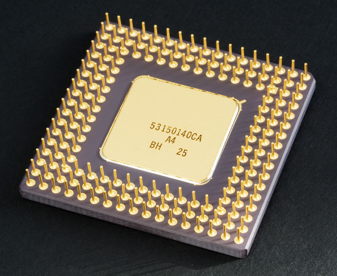

Questions people ask about Intel 486DX2
What does the DX2 name mean?
It marks a 486 whose internal clock runs at twice the speed of the external bus. A board running its bus at 25 MHz could therefore host a core at 50 MHz, or 33 MHz paired with 66 MHz.
How much faster was it than a plain 486DX?
Depending on the application, the multiplier delivered around 50 to 70 percent more performance than a 486DX on the same external bus. Dhrystone V1.1 measured 40 MIPS for the 50 MHz part and 54 MIPS for the 66 MHz one.
What is the difference between P24 and P24D?
P24 is the first revision and can only use write-through caching, where each store goes on to main memory. P24D adds write-back mode, keeping updated data in the level-one cache and so raising performance.
Was there a low-power version?
Yes. Intel prepared a 3.3 volt, 50 MHz model with System Management Mode. It drew 1.5 watts, less than 60 percent of the equivalent 5 volt chip, and used a 208-lead SQFP package that saved board space and volume.
Good reading and sources
The facts on this page come from the Wikipedia article "Intel DX2", written by its contributors and used under the CC BY-SA 4.0 licence, and from its Wikidata record (CC0). EveryChip rewrote the text in its own words, with AI assistance, and compares every page with the article to make sure no passage is copied. It may be reused under the same CC BY-SA 4.0 licence with a link back.
It may contain mistakes, and figures change over time. Nothing here is investment or buying advice. If something is wrong, tell us. Last refreshed 2026-11-14.
Like Intel 486DX2
All CPUs and microprocessors 🇺🇸 United StatesPowerPC 600
Early PowerPC processor family for PCs, workstations and embedded gearCPU · Power · 1993
 🇺🇸 United StatesAm386
AMD's first independent x86 microprocessor cloneCPU · x86 · 1991
 🇺🇸 United StatesIntel 80486SX
A 1991 Intel 486 CPU sold without a working floating-point unitCPU · x86 · 1991
 🇺🇸 United StatesPentium
Intel's first superscalar x86 chip, with dual integer pipelines and a faster FPUCPU · x86 · 1993
More from Intel
All of them 🇺🇸 United StatesDEC Alpha
A 64-bit RISC architecture by Digital Equipment CorporationCPU · RISC · 1992
 🇺🇸 United StatesRealityEngine
High-end 3D graphics hardware by Silicon GraphicsGPU · Other · 1992
 🇺🇸 United StatesPentium
Intel's long-running x86 processor brand, from the 1993 P5 to 2023 budget partsCPU · x86 · 1993
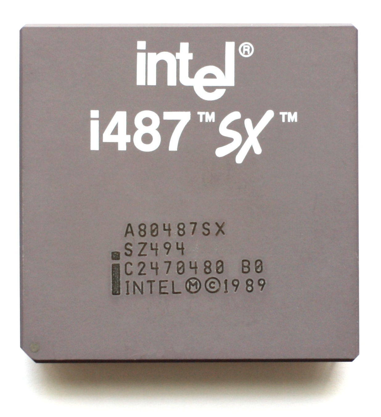 🇺🇸 United StatesIntel 80487SX
Floating-point upgrade chip for Intel 486SX systemsCPU · x86 · 1991