
Intel 8085
An 8-bit Intel microprocessor from 1976, the last of its line
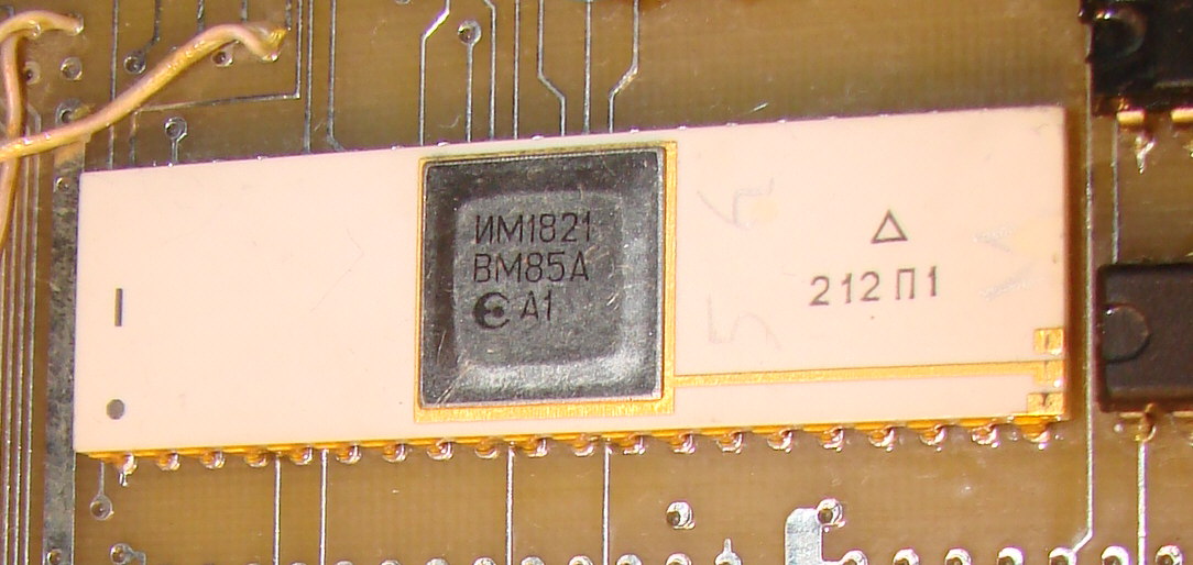
The Intel 8085 is an 8-bit microprocessor that Intel introduced in March 1976 as a follow-up to the 8080. It runs the same machine code as the 8080 but needs only one 5 V supply and adds serial and interrupt pins, which kept it in production for decades in control equipment.
- Introduced March 1976; Intel's last 8-bit microprocessor
- Runs 8080 binary code unchanged, apart from the AND/ANI flag detail
- Needs only a single +5 V supply
- About 6,500 transistors in a 40-pin DIP
- SIM and RIM instructions finish in four clock cycles
What it is
This is an 8-bit central processing unit built by Intel and put on sale in March 1976. It executes the same binary programs as the earlier Intel 8080, so existing code could move across without rewriting. The digit 5 in its name signals the single +5 V supply it needs, whereas the 8080 required three rails. Four interrupt inputs and a serial port with its own send and receive pins were folded onto the chip, cutting the number of companion circuits a small design required. It became Intel's final 8-bit processor design.
How it came about
Intel brought the part out in March 1976 as a tidied-up successor to the 8080. Designers at the time already judged it weaker than rival chips on the market, and work on the 16-bit 8086 was under way. Late in the programme Intel chose to leave ten of twelve added instructions out of the official documentation, easing the job of building the 8086. Two software engineers, Wolfgang Dehnhardt and Villy M. Sorensen, later uncovered those hidden instructions while writing an assembler.
Inside the chip
A von Neumann layout inherited from the 8080: one bus carries both instructions and data. Seven 8-bit registers (A, B, C, D, E, H, L) sit inside, with A acting as the accumulator, plus a program counter and a stack pointer. The lower half of the address bus shares pins with the data bus, so a full 16-bit address travels in two byte-wide stages and one stage must be held by an external latch such as a 74LS373. Five interrupt lines, a serial pair, and on-chip clock and system-control functions replace several outside chips. SIM and RIM, the only genuinely new instructions, handle interrupt masks and serial traffic in four clock cycles.
How it was made
Roughly 6,500 transistors were built with nMOS circuitry; later H-marked parts used Intel's HMOS II process, a technology first created for fast static RAM. The die is listed at 3 µm. Intel fabricated the device and other firms produced it as well. Packaging is a 40-pin dual in-line case, with pin 40 for +5 V, pin 20 for ground and pin 39 for Hold.
Where it went
The chip rarely powered full desktop computers. Instead it served long stretches inside control hardware, notably the DECtape II controller and the VT102 video terminal from the late 1970s, and stayed in fresh production for as long as those products sold. Paired with Intel memory parts carrying built-in address latches, it formed nearly a whole small system.
Versions and family
It came after the Intel 8080 and before the Intel 8086. H-suffix versions used the faster HMOS II process. Companion chips such as the 8755 (2 KB EPROM, 16 I/O lines, built-in latch) and the 8155 (256 bytes RAM, 22 I/O lines, 14-bit timer/counter) were made to match it. The Zilog Z80 overtook it in the home computer arena during the late 1970s and early 1980s.
Why it matters
By folding clock generation and bus control onto one die and running from a single rail, the 8085 showed how far integration could shrink a small system. Its instruction set and pin ideas carried into later Intel work, and its long service life in terminals and controllers kept it relevant well past the era of 8-bit desktop machines.
Problems and reception
Engineers of the period saw the design as behind its competitors even before launch. The Z80 took most of the desktop market from it. Hidden opcodes and undocumented flags caused confusion until they were traced by Denhardt and Sorensen, and at least one second-source maker published details of them.


Questions people ask about Intel 8085
What does the 5 in 8085 stand for?
It marks the single +5 V supply the chip uses. The older 8080 needed +5 V, −5 V and +12 V, so the 8085 dropped into the 5 V systems common by then with far less extra circuitry.
Can it run programs written for the 8080?
Yes. It executes the full 8080 instruction set with matching behaviour, so most 8080 object code runs untouched. Timing differs slightly, and the AND/ANI flag handling is one exception.
Why does the address bus share pins with data?
The 40-pin package had no room for separate buses once new interrupt and serial pins were added. The low eight address bits share lines with data, so an address is sent in two byte stages and one stage is latched outside the chip.
What is special about SIM and RIM?
They are the only instructions not inherited from the 8080. Each runs in four clock cycles and controls interrupt masks, reads pending interrupt states, and moves serial data through the SOD and SID pins.
What replaced it?
Intel's 16-bit 8086 succeeded it in the product line, while the Zilog Z80 took over much of the desktop computer market in the late 1970s and early 1980s.
Good reading and sources
The facts on this page come from the Wikipedia article "Intel 8085", written by its contributors and used under the CC BY-SA 4.0 licence, and from its Wikidata record (CC0). EveryChip rewrote the text in its own words, with AI assistance, and compares every page with the article to make sure no passage is copied. It may be reused under the same CC BY-SA 4.0 licence with a link back.
It may contain mistakes, and figures change over time. Nothing here is investment or buying advice. If something is wrong, tell us. Last refreshed 2026-11-14.
Like Intel 8085
All CPUs and microprocessors 🇺🇸 United StatesSignetics 2650
8-bit microprocessor from 1975 modelled on the IBM 1130 minicomputerCPU · 8-bit · 1975
 🇺🇸 United StatesFairchild F8
An early 8-bit microprocessor family built for small controller jobsCPU · 8-bit · 1974
 🇺🇸 United StatesIntel 80186
16-bit microprocessor with integrated peripherals for embedded systemsCPU · x86 · 1982
 🇺🇸 United StatesWDC 65C02
CMOS rework of the 6502 with lower power and extra instructionsCPU · 8-bit · 1983
More from Intel
All of them 🇺🇸 United StatesIntel 8259
Programmable interrupt controller for early Intel microprocessorsAnalog · Other · 1976
 🇺🇸 United StatesMCS-48
Intel's first microcontroller series from 1976Microcontroller · Other · 1976
 WorldFloppy disk controller
Chip that manages reading and writing data to floppy disksAnalog · 1976
 🇺🇸 United StatesIntel 8251
Universal synchronous and asynchronous receiver transmitter chip by IntelNetwork chip · Other · 1975