
Apple A15 Bionic
Six-core ARM system on a chip for Apple mobile devices
Apple designed this six-core processor using TSMC manufacturing. It powers several iPhones and iPads starting in late 2021. The chip integrates graphics and neural processing units for mobile tasks.
- Contains 15 billion transistors on a 5 nm process
- Features two Avalanche and four Blizzard CPU cores
- Includes a 16-core Neural Engine for AI tasks
- Debuted in the iPhone 13 series in September 2021
What it is
This integrated circuit combines central processing, graphics, and machine learning hardware on one silicon die. Apple created the design for its mobile product line. TSMC fabricated the chips using a five-nanometre process. The component debuted in September 2021 inside the iPhone 13 lineup. It serves as the main computing engine for several smartphones and tablets, handling everyday tasks and heavy graphical workloads efficiently.
How it came about
Engineers at Apple developed this successor to the A14 Bionic. They aimed to boost speed and efficiency for mobile devices. The team increased the transistor count significantly compared to the prior generation. Production began in late 2021. The chip first appeared in the iPhone 13 models and the sixth-generation iPad Mini. Later releases included the third-generation iPhone SE and the fourteenth-generation iPhones.
Inside the chip
The processor uses two distinct core types. Two high-performance cores, named Avalanche, run at speeds up to 3.23 GHz. Four efficiency cores, called Blizzard, handle lighter tasks to save power. A dedicated sixteen-core Neural Engine processes machine learning operations rapidly. The system includes a thirty-two-megabyte shared cache. Graphics processing comes from either a four-core or five-core GPU, depending on the specific device model.
How it was made
TSMC manufactured the silicon wafers using its N5P fabrication technique. This second-generation five-nanometre process allowed for fifteen billion transistors on the die. This count represents a substantial increase over the previous A14 chip. The compact design enables high performance within the thermal limits of small handheld devices. Apple oversaw the architectural design while TSMC handled the physical production.
Where it went
Smartphones such as the iPhone 13, 13 Pro, 14, and 14 Plus rely on this chip. The third-generation iPhone SE also uses it. Tablet users find it in the sixth-generation iPad Mini. The third-generation Apple TV 4K streaming box contains a variant with one efficiency core disabled. These devices benefit from improved video encoding and computational photography features provided by the hardware.
Versions and family
Models differ mainly in their graphics configuration. The iPhone 13 and iPhone SE use a four-core GPU. Pro models and the iPad Mini include a five-core GPU. The iPad Mini version runs its performance cores at a slightly lower clock speed. The Apple TV variant disables one efficiency core. This chip follows the A14 Bionic and precedes the A16 Bionic in the product lineage.
Why it matters
The component delivered notable performance gains over its predecessor. Single-core frequencies increased, enhancing responsiveness for user interfaces. The neural engine saw a large jump in operational throughput. These improvements supported advanced camera features and smoother gaming experiences. It maintained Apple's strategy of custom silicon for its ecosystem, reducing reliance on third-party suppliers for core logic.
Problems and reception
Technical analyses highlighted the frequency boosts in the performance cluster. Reviewers noted the efficiency gains from the new core design. The increased transistor budget allowed for better sustained performance. Users experienced faster app loading and improved battery life in compatible devices. The chip was widely regarded as a strong step forward in mobile processing capability.
Questions people ask about Apple A15 Bionic
What devices use the Apple A15 Bionic?
This chip powers the iPhone 13 series, iPhone 14 standard models, iPhone SE third generation, iPad Mini sixth generation, and Apple TV 4K third generation. Each device may use a slightly different configuration of the graphics or CPU cores.
How many cores does the processor have?
It has six central processing cores in total. Two are high-performance Avalanche cores for demanding tasks. Four are energy-efficient Blizzard cores for background activities and light usage. This mix helps balance speed and battery life.
Who manufactures the Apple A15 Bionic?
Apple Inc. designs the architecture and logic of the chip. TSMC is the foundry that physically manufactures the silicon wafers. They use a five-nanometre process known as N5P to produce the components.
What is the clock speed of the A15?
The performance cores can reach speeds up to 3.23 GHz in most iPhones. In the iPad Mini sixth generation, the speed is limited to 2.93 GHz. The efficiency cores operate at lower frequencies to conserve power during simple tasks.
Good reading and sources
- Checking your browserAnandTech, Article
- Apple A15 Bionic Powers iPhone 13 and iPad MiniTom's Hardware, Article
The facts on this page come from the Wikipedia article "Apple A15", written by its contributors and used under the CC BY-SA 4.0 licence, and from its Wikidata record (CC0). EveryChip rewrote the text in its own words, with AI assistance, and compares every page with the article to make sure no passage is copied. It may be reused under the same CC BY-SA 4.0 licence with a link back.
It may contain mistakes, and figures change over time. Nothing here is investment or buying advice. If something is wrong, tell us. Last refreshed 2026-11-14.
Like Apple A15 Bionic
All systems on a chip 🇺🇸 United StatesApple A14 Bionic
Apple's 5 nm phone and tablet chip with six CPU cores and a 16-core Neural EngineSoC · Arm · 2020
 🇺🇸 United StatesApple M2
Apple's second-generation ARM SoC family for Macs, iPads and Vision ProSoC · Arm · 2022
 🇺🇸 United StatesApple A13 Bionic
64-bit ARM system on a chip for mobile devicesSoC · Arm · 2019
 🇺🇸 United StatesApple U1
Ultra-wideband system on a chip for spatial awarenessSoC · Arm · 2019
More from Apple Inc.
All of them 🇬🇧 United KingdomRP2040
Dual-core ARM Cortex-M0+ microcontroller by Raspberry PiMicrocontroller · Arm · 2021
 🇺🇸 United StatesApple M1 Pro
Professional ARM system-on-a-chip for Mac laptopsSoC · Arm · 2021
🇺🇸 United StatesApple M1 Max
High-performance ARM system-on-a-chip for professional MacsSoC · Arm · 2021
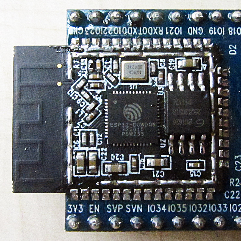 🇨🇳 ChinaESP32
Low-cost Wi-Fi and Bluetooth microcontroller family by EspressifMicrocontroller · RISC · 2021