
Tejas and Jayhawk
Cancelled Intel CPU cores planned as successors to Prescott Pentium 4 and Xeon
Tejas was Intel's planned successor to the Prescott-core Pentium 4, with Jayhawk as its Xeon counterpart. Cancelled on 7 May 2004 before release, the pair marked the point where Intel abandoned ever-higher single-core clock speeds and turned toward multi-core designs.
- Cancelled by Intel on 7 May 2004
- Planned pipeline of 40 to 50 stages
- Targets reached 7 GHz and beyond, with 10 GHz eyed for 2011
- Reported 2.8 GHz samples rated at 150 W on LGA 775
- Its end pushed Intel from single-core to multi-core designs
What it is
Tejas was the code name for a microprocessor Intel intended as the next step after the Prescott-core Pentium 4, and it was sometimes called Pentium V. Jayhawk covered the matching Xeon part. Neither chip shipped. Intel cancelled both on 7 May 2004, and the decision became a clear marker of the company's move away from single-core designs chasing ever higher clock speeds and toward multi-core processors instead.
How it came about
Intel previewed Tejas in early 2003, with a launch pencilled in for 2004 and possible slip into 2005. Development was halted on 7 May 2004. Analysts pointed to heat and power draw as the core problem, the result of pushing frequency harder while gaining little work per clock. Prescott had already shown this pattern, barely beating Northwood despite running faster, and AMD's Athlon 64 pressed hard. Intel had talked of 10 GHz by 2011, echoing Andrew Grove's 1996 COMDEX keynote, but the approach proved a dead end.
Inside the chip
Tejas and Jayhawk were meant to extend the NetBurst design used in the Pentium 4. The plan called for a 90 nm part first, then a 65 nm shrink, with L2 cache rising from 1 MB to 2 MB. The trace cache would likely grow, and the pipeline would stretch to between 40 and 50 stages, a long chain of execution steps that lets the chip run fast but wastes work on mispredicted branches. An improved Hyper-Threading and a new SSE version were planned; that SSE extension later appeared in Core 2 as SSSE3. Frequencies of 7 GHz or more were targeted, though performance would not have scaled linearly.
How it was made
Tejas was to start on a 90 nm process and later move to 65 nm. Reports described early single-core 90 nm samples at 2.8 GHz with a 150 W rating on the LGA 775 socket, well above the 84 W of a comparable Prescott and the 95 W of the dual-core Smithfield. The project was cancelled late, after what was described as tapeout. Those sample claims have since been disputed, and the pictured part was identified as a Prescott B0 engineering sample; only thermal samples of Tejas are now thought to have been made.
Where it went
Tejas and Jayhawk never reached products. They were aimed at desktops as the Pentium 4 successor and at servers as the Xeon counterpart. After cancellation, Intel filled the gap with one final NetBurst revision: Cedar Mill for single core and Presler for dual core.
Versions and family
A dual-core Tejas was planned under the name Cedarmill, distinct from the later 65 nm Cedar Mill Pentium 4 that reused the codename. Jayhawk was the Xeon sibling. The line ended with Cedar Mill and Presler, while Intel's desktop work moved to the Pentium M lineage and then Core and Core 2.
Why it matters
Cancelling Tejas and Jayhawk closed out the NetBurst era. Intel shifted desktop development to the Pentium M microarchitecture, a P6 derivative from the Centrino notebooks, which delivered far better performance per watt. Modernising that design produced Core and then Core 2, Intel's first native dual-core desktop and laptop chips, which took the performance lead back from AMD. NetBurst ideas were later revisited in Sandy Bridge.
Problems and reception
The cancellation drew wide attention as the end of the clock-speed race. Claims about working Tejas samples have been challenged, with the part shown in one report identified as a Prescott B0 engineering sample, and no confirmed tapeout. Most likely only thermal samples were ever produced.
Questions people ask about Tejas and Jayhawk
What were Tejas and Jayhawk?
Tejas was the code name for an Intel microprocessor planned as the successor to the Prescott-core Pentium 4, sometimes called Pentium V. Jayhawk was the matching Xeon version. Both were cancelled in May 2004 and never sold.
Why were they cancelled?
Heat and power draw were the main issues. Intel was chasing ever higher clock speeds while gaining little work per clock, and Prescott had already shown weak gains over Northwood. AMD's Athlon 64 added pressure. The path to 10 GHz proved a dead end.
What did Intel do instead?
It moved desktop work to the Pentium M microarchitecture, derived from P6 and used in Centrino, which gave much better performance per watt. That line led to Core and Core 2, Intel's first native dual-core desktop and laptop chips. Cedar Mill and Presler were the last NetBurst parts.
Were any Tejas chips actually built?
Reports of early 2.8 GHz samples at 150 W have been disputed. The sample shown in one report was identified as a Prescott B0 engineering sample, and no confirmed tapeout exists. Most likely only thermal samples of Tejas were produced.
Good reading and sources
- Checking your browserAnandTech, Article
- Intel product specificationsIntel, Article
- Intel’s Netburst: Failure is a Foundation for SuccessChips and Cheese, Article
The facts on this page come from the Wikipedia article "Tejas and Jayhawk", written by its contributors and used under the CC BY-SA 4.0 licence, and from its Wikidata record (CC0). EveryChip rewrote the text in its own words, with AI assistance, and compares every page with the article to make sure no passage is copied. It may be reused under the same CC BY-SA 4.0 licence with a link back.
It may contain mistakes, and figures change over time. Nothing here is investment or buying advice. If something is wrong, tell us. Last refreshed 2026-11-14.
Like Tejas and Jayhawk
All CPUs and microprocessors 🇺🇸 United StatesTigerton
Intel Xeon processor model released in 2005 for servers.CPU · x86 · 2005
 🇺🇸 United StatesYonah
Intel's first 65 nm mobile CPU cores, sold as Core Duo and Core SoloCPU · x86 · 2006
 🇺🇸 United StatesIntel Core
Intel's multi-core x86 CPU line for laptops, desktops and workstationsCPU · x86 · 2006
 🇮🇱 IsraelIntel Core microarchitecture
Intel's 2006 multi-core CPU design that replaced NetBurst across desktops, laptops and serversCPU · x86 · 2006
More from Intel
All of them 🇺🇸 United StatesIntel GMA
Integrated graphics series for low-cost PCs by IntelGPU · GPU architecture · 2004
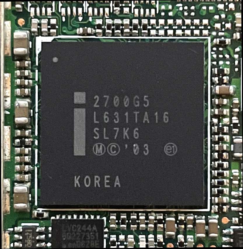 🇺🇸 United StatesIntel 2700G
Mobile graphics co-processor for XScale PXA27xGPU · GPU architecture · 2004
 🇺🇸 United StatesPentium D
Intel's first dual-core desktop Pentium, two NetBurst cores in one packageCPU · x86 · 2005
 🇺🇸 United States and 1 morePentium M
Intel's power-saving laptop CPU line, launched in 2003 on the P6 designCPU · x86 · 2003