
GDDR5 SDRAM
High-bandwidth graphics memory for cards and consoles
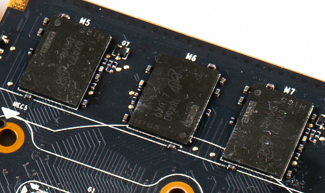
GDDR5 SDRAM is a synchronous graphics memory standard developed by JEDEC for high-performance visual computing. It succeeded GDDR4 and powers graphics cards, game consoles like the PlayStation 4, and high-performance systems with fast data transfer rates.
- First shipped by AMD in June 2008
- Used in PlayStation 4 with 8 GB total
- Samsung mass-produced 8 Gb chips in 2015
- Operates with three distinct clock signals
- Standardized by JEDEC as fifth generation
What it is
GDDR5 SDRAM is a type of synchronous graphics random-access memory designed for high bandwidth applications. It serves as the primary video memory for graphics cards, game consoles, and high-performance computing systems. The standard was defined by JEDEC and builds upon DDR3 SDRAM technology. It uses an 8N-prefetch architecture to achieve fast data transfer rates. This memory type allows graphics processors to handle large frame buffers and complex rendering tasks efficiently.
How it came about
Samsung Electronics revealed GDDR5 in July 2007 and began mass production in January 2008. Hynix Semiconductor introduced the first 1 Gb chips in 2007 using a 60 nm process. AMD became the first company to ship products with this memory in June 2008, using modules from Qimonda. Elpida Memory later established a design centre in Munich after acquiring assets from Qimonda. Micron Technology eventually acquired Elpida and continued development of higher density chips.
Inside the chip
The interface transfers two 32-bit data words per write clock cycle. It operates with three clocks: one command clock and two write clocks. The command clock runs at half the frequency of the write clocks. This alignment minimises latency during read and write operations. The memory can operate in 32-bit or 16-bit clamshell modes. A single 32-bit chip uses a 170-ball grid array package with about 67 signal pins. The rest of the pins are for power and ground connections.
How it was made
Manufacturers used various process nodes, starting from 60 nm and shrinking to 20 nm. Samsung began mass producing 8 Gb chips on a 20 nm process in 2015. Micron also started commercial shipments of 8 Gb components using 20 nm technology in early 2015. Hynix produced 2 Gb chips on a 40 nm class process in 2010. Qimonda demonstrated volume production of 512 Mb components in 2008. The packaging typically involves a 170-pin ball grid array for standard GDDR5.
Where it went
This memory is found in graphics cards such as the AMD Radeon HD 4870 and Nvidia GeForce GTX 980 Ti. It was selected for the PlayStation 4 console, which uses sixteen 4 Gb chips for a total of 8 GB. The high bandwidth supports 4K displays and graphically intensive PC gaming. It is also used in high-performance computing applications that require rapid data access. The memory serves as both system and graphics RAM in some console architectures.
Versions and family
GDDR5X is a standardized variant that offers double the transfer rate per pin. It uses a 190-pin package instead of the standard 170 pins. GDDR5X supports quad data rate mode with a 16n prefetch. Standard GDDR5 was succeeded by GDDR6. Predecessors include GDDR4 SDRAM. Chip densities increased from 512 Mb to 8 Gb over time. Manufacturers released 1 Gb, 2 Gb, 4 Gb, and 8 Gb versions sequentially.
Why it matters
GDDR5 enabled higher resolution gaming and more complex graphical effects. It allowed consoles like the PlayStation 4 to use unified memory architectures. The shift to 20 nm processes increased density and bandwidth significantly. It became the standard for mid-to-high-end graphics cards for several years. The technology supported the mainstream adoption of 4K displays by providing necessary frame buffer capacity.

Questions people ask about GDDR5 SDRAM
What is GDDR5 memory used for?
It is designed for graphics cards, game consoles, and high-performance computing. It provides the high bandwidth needed for rendering complex images and handling large frame buffers in gaming and professional applications.
Who developed the GDDR5 standard?
The JEDEC Solid State Technology Association developed the standards for GDDR5 SDRAM. Major manufacturers like Samsung, Hynix, and Qimonda contributed to its commercialization and production.
How does GDDR5 differ from GDDR5X?
GDDR5X offers twice the transfer rate per pin and uses a 190-pin package. It supports quad data rate mode, whereas standard GDDR5 uses double data rate mode with a 170-pin package.
Good reading and sources
- A Quantum Leap in Gaming: NVIDIA Introduces GeForce GTX 1080Nvidia, Article
- Checking your browserAnandTech, Article
The facts on this page come from the Wikipedia article "GDDR5 SDRAM", written by its contributors and used under the CC BY-SA 4.0 licence, and from its Wikidata record (CC0). EveryChip rewrote the text in its own words, with AI assistance, and compares every page with the article to make sure no passage is copied. It may be reused under the same CC BY-SA 4.0 licence with a link back.
It may contain mistakes, and figures change over time. Nothing here is investment or buying advice. If something is wrong, tell us. Last refreshed 2026-11-14.
Like GDDR5 SDRAM
All memory chips WorldGDDR6 SDRAM
High-bandwidth graphics memory for GPUs and consolesMemory · 2017
 WorldGDDR SDRAM
High-bandwidth synchronous memory designed for graphics processors.Memory · 1998
 🇰🇷 South KoreaDDR SDRAM
First generation double data rate memory standard for computers.Memory · 1998
 WorldGDDR7 SDRAM
High-bandwidth graphics memory standard for GPUs and computing.Memory · 2024
More from JEDEC
All of them WorldDDR3 SDRAM
Third-generation double data rate memory standard released in 2007Memory · 2007
 🇰🇷 South KoreaExynos
Samsung's Arm-based system-on-chip series for phones, wearables, cars and IoTSoC · Arm · 2009
 🇬🇧 United KingdomARM Cortex-A9
32-bit multi-core processor core for mobile and embedded systemsCPU · Arm · 2007
 🇺🇸 United StatesApple A4
Apple's first in-house SoC: one Cortex-A8 core plus PowerVR graphics, built at 45 nm.SoC · Arm · 2010