
Espresso
32-bit PowerPC CPU for the Nintendo Wii U console
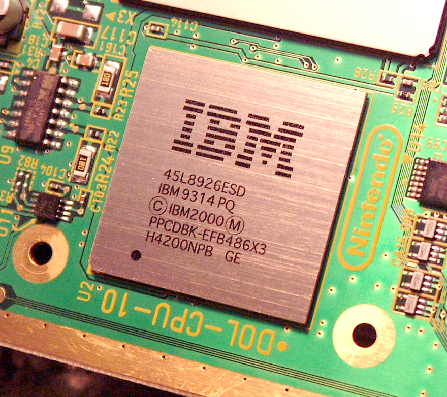
Espresso is a 32-bit central processing unit designed by IBM for Nintendo's Wii U video game console. Released in November 2012, it uses a triple-core PowerPC architecture on a 45 nm process to balance performance and power efficiency within a multi-chip module.
- Triple-core PowerPC CPU running at 1.243 GHz
- Manufactured by IBM using 45 nm SOI process
- Features 3 MB of on-die L2 cache in asymmetric layout
- Part of a multi-chip module with AMD Latte GPU
- Used exclusively in the Nintendo Wii U console
What it is
Espresso is the central processing unit found inside the Nintendo Wii U home video game console. IBM designed this 32-bit chip using PowerPC technology, specifically basing it on the PowerPC 750CL microarchitecture. The processor features three cores and was manufactured using a 45 nanometre silicon-on-insulator process. It operates as part of a larger multi-chip module that includes graphics hardware from AMD. Nintendo revealed the system in mid-2011, with the console launching in late 2012. The design prioritises low power consumption and compact size over raw server-class performance.
How it came about
IBM and Nintendo collaborated to create a processor that improved upon the earlier Broadway chip used in the original Wii. The team focused on reducing manufacturing costs and physical space requirements while boosting speed. They chose to keep the core architecture similar to previous generations to maintain backward compatibility. This approach avoided the high expenses associated with adopting high-end server processors like the POWER7. The chip was assembled into a multi-chip module by Renesas in Japan before being integrated into the final console hardware released in November 2012.
Inside the chip
The processor contains three symmetric cores running at approximately 1.243 GHz. Each core supports superscalar parallelism, allowing it to issue up to four instructions per clock cycle. The integer units are 32-bit, while the floating-point units handle 64-bit operations or two 32-bit SIMD instructions. A distinctive feature is the uneven distribution of its 3 MB Level 2 cache. One core receives 2 MB of cache, while the other two share the remaining 1 MB equally. This on-die cache uses embedded DRAM technology. The pipeline depth is four stages for integer operations and seven stages for floating-point tasks.
How it was made
IBM manufactured the Espresso die at its 300 mm facility in East Fishkill, New York. The production used 45 nm silicon-on-insulator technology, which helps reduce leakage current and power usage. The individual CPU die measures roughly 27.73 square millimetres. After fabrication, the chip was combined with an AMD graphics processor and a small EEPROM memory chip. Renesas assembled these components onto a single substrate to form the multi-chip module. This packaging method simplifies the motherboard layout and improves communication speeds between the CPU and GPU.
Where it went
This processor serves exclusively as the main brain for the Nintendo Wii U video game console. It handles game logic, physics calculations, and system operations for all software titles on the platform. The chip’s architecture allows it to run games developed for the previous Wii console, ensuring a library of legacy titles remains playable. Its integration into a multi-chip module means it works closely with the Latte graphics processor to render visuals. No other consumer electronic devices or computers utilise this specific custom silicon design.
Versions and family
Espresso has no official commercial variants or different speed bins. It is a single custom design made specifically for one hardware platform. Its direct predecessor is the Broadway processor, which powered the original Wii. Both chips share a lineage tracing back to the Gekko processor from the GameCube era. The successor to the Espresso in Nintendo’s hardware lineup is the Nvidia Tegra X1, codenamed Erista, which powers the Switch console. There were rumours of a link to IBM’s POWER7 servers, but these were confirmed to be false.
Why it matters
The chip demonstrated how console manufacturers could use mature, cost-effective processes to deliver adequate performance. By sticking with a known PowerPC architecture, Nintendo ensured developers could port existing code easily. The use of a multi-chip module set a precedent for integrating CPU and GPU components tightly to save space. While not powerful enough to compete with contemporary personal computers, it provided a stable platform for exclusive first-party games. The design choices reflected a priority on energy efficiency and manufacturing economy over peak computational throughput.
Problems and reception
Technical details were not officially published by Nintendo or IBM at launch. Enthusiasts and hackers later reverse-engineered the hardware to reveal specifications such as clock speeds and cache sizes. Some critics initially worried the processor was underpowered compared to rival home consoles. However, the confirmation that it was not a repurposed server chip alleviated concerns about excessive cost or heat. The community generally accepted the hardware limitations as a trade-off for the unique gameplay features offered by the Wii U tablet controller.


Questions people ask about Espresso
What architecture does the Espresso CPU use?
It uses a 32-bit PowerPC architecture based on the PowerPC 750CL microarchitecture. This design is similar to the earlier Broadway and Gekko processors, ensuring backward compatibility with older software while adding multiprocessor support.
How many cores does the Espresso processor have?
The chip contains three processing cores. They operate at a clock speed of approximately 1.243 GHz. Each core can execute multiple instructions per cycle using superscalar parallelism to improve overall throughput.
Who manufactured the Espresso chip?
IBM designed and manufactured the CPU die at its plant in East Fishkill, New York. The final multi-chip module, which includes the CPU, GPU, and memory, was assembled by Renesas in Japan.
Is the Espresso CPU related to IBM POWER7 servers?
No. Although it shares some superficial technologies like embedded DRAM, it is not derived from the POWER7 server line. It is based on the older PowerPC 750 family to keep costs and size down for a consumer console.
Good reading and sources
- Espresso (processor) on WikipediaEncyclopedia
- More photos on Wikimedia CommonsPhotos
- Wikidata recordOpen data
The facts on this page come from the Wikipedia article "Espresso (processor)", written by its contributors and used under the CC BY-SA 4.0 licence, and from its Wikidata record (CC0). EveryChip rewrote the text in its own words, with AI assistance, and compares every page with the article to make sure no passage is copied. It may be reused under the same CC BY-SA 4.0 licence with a link back.
It may contain mistakes, and figures change over time. Nothing here is investment or buying advice. If something is wrong, tell us. Last refreshed 2026-11-14.
Like Espresso
All CPUs and microprocessors 🇺🇸 United StatesBroadway
32-bit PowerPC CPU for the Nintendo Wii consoleCPU · Power · 2006
 🇺🇸 United States and 1 moreMicrosoft XCPU (Xenon)
Three-core PowerPC CPU at the heart of the Xbox 360 consoleCPU · Power · 2003
 🇺🇸 United StatesGekko
Custom PowerPC CPU for the Nintendo GameCubeCPU · Power · 2000
 🇺🇸 United StatesPowerPC 7xx
Third-generation 32-bit PowerPC microprocessor family for PCs and embedded systems.CPU · Power · 1997
More from IBM
All of them 🇺🇸 United States and 1 moreLatte
AMD Radeon-based graphics chip for the Nintendo Wii U consoleGPU · GPU architecture · 2012
🇺🇸 United StatesZEC12
IBM mainframe processor with 5.5 GHz clock speedCPU · Other · 2012
🇺🇸 United StatesIBM A2
Open source 64-bit Power ISA processor core for embedded systemsCPU · Power · 2010
 🇺🇸 United StatesPOWER8
IBM multi-core server processor with OpenPOWER licensingCPU · Power · 2014