
Kepler
Nvidia GPU microarchitecture focused on energy efficiency and programmability.
Kepler is a graphics processing unit design by Nvidia, launched in April 2012. It succeeded Fermi and prioritised power efficiency over raw clock speed increases. Manufactured by TSMC on a 28 nm process, it powered GeForce 600 and 700 series cards. The architecture introduced features like GPU Boost and Dynamic Parallelism to improve performance per watt.
- First Nvidia architecture to prioritise energy efficiency
- Introduced GPU Boost for dynamic clock scaling
- Manufactured on TSMC 28 nm process node
- Supports DirectX 12 feature level 11_0
- Features Hyper-Q with 32 hardware work queues
What it is
Kepler is a graphics processor microarchitecture created by Nvidia. It reached retail markets in April 2012 as the successor to the Fermi design. This generation marked a strategic shift for the company, moving away from pure performance gains to focus on energy efficiency and programmability. Built on a 28 nanometre manufacturing process by TSMC, Kepler chips powered the GeForce 600 and 700 series, along with professional Quadro and Tesla computing modules. The architecture is named after the German mathematician Johannes Kepler.
How it came about
Nvidia developed Kepler to address the power consumption issues of its predecessor, Fermi. While Fermi prioritised compute and tessellation performance, Kepler aimed to balance performance with efficiency. The design team simplified instruction scheduling and removed complex hardware blocks that prevented data hazards. This reduction in die space helped lower power usage. The architecture was first introduced in April 2012 and remained in production alongside its successor, Maxwell, in later GeForce series.
Inside the chip
Kepler uses a new streaming multiprocessor called SMX. Each SMX contains 192 CUDA cores, a significant increase from the 32 cores per unit in Fermi. The design employs a unified GPU clock rather than separate shader clocks, which reduces power consumption by half in that area. Key features include Hyper-Q, which expands work queues to 32 to improve utilisation, and Dynamic Parallelism, allowing kernels to dispatch other kernels without CPU involvement. The GK110 variant supports double-precision calculations at one-third the speed of single-precision, while consumer models are limited to one-twenty-fourth.
How it was made
TSMC manufactured all Kepler chips using its 28 nm process node. The architecture includes various dies such as GK10x, GK110, and GK210. The GK210 increased register limits to 512 to handle high register pressure situations. Memory support includes GDDR5 with speeds up to 7 GHz. The design incorporates single-bit error correction code for all memory levels, including the register file. Video encoding is handled by the NVENC block, which supports H.264 content up to 4K resolution.
Where it went
Kepler GPUs were widely used in desktop gaming PCs through the GeForce 600 and 700 series. They also powered professional workstations via the Quadro K series and high-performance computing clusters through Tesla K modules. The GK20A variant served as the graphics component in the Tegra K1 system on a chip. Features like GPU Boost allowed these cards to dynamically adjust clock speeds based on thermal headroom, maximising performance within power limits. The architecture supports DirectX 12 feature level 11_0 and Vulkan 1.2.
Versions and family
The Kepler family includes several variants. Consumer cards mostly use GK10x dies with limited double-precision performance. High-end computing cards like the GK110 and GK210 offer improved double-precision ratios and more streaming multiprocessors. The GK208 and GK20A represent smaller or embedded implementations. Kepler was succeeded by the Maxwell microarchitecture, though some GeForce 800M series laptops used Kepler chips alongside newer Maxwell designs. The architecture is now unsupported by Nvidia.
Why it matters
Kepler established energy efficiency as a primary goal for Nvidia GPU design. Its introduction of GPU Boost changed how graphics cards manage power, allowing dynamic frequency scaling similar to central processing units. Features like Hyper-Q and Dynamic Parallelism improved software flexibility for high-performance computing tasks. The architecture supported advanced video decoding for H.265 and encoding for H.264, enabling efficient media processing. It laid the groundwork for future efficiency-focused designs like Maxwell and Pascal.


Questions people ask about Kepler
What is the main difference between Kepler and Fermi?
Kepler focuses on energy efficiency and programmability, whereas Fermi prioritised raw performance in compute and tessellation. Kepler uses a unified GPU clock and simplified scheduling to reduce power consumption, achieving better performance per watt than its predecessor.
Which products used the Kepler microarchitecture?
Kepler powered the Nvidia GeForce 600 and 700 series graphics cards. It was also used in the Quadro K series for workstations, Tesla K modules for servers, and the GK20A chip inside the Tegra K1 system on a chip for mobile devices.
What is GPU Boost in Kepler GPUs?
GPU Boost is a feature that dynamically adjusts the graphics card clock speed. It ensures the GPU runs at a base clock but increases speed when thermal and power limits allow. This maximises performance without exceeding the specified power target, typically 170 W for reference cards.
Does Kepler support modern graphics APIs?
Yes, Kepler GPUs support DirectX 12 up to feature level 11_0 and Vulkan 1.2. They also support OpenGL 4.6. However, they do not support all DirectX 11.1 features, such as target-independent rasterisation, which limits their compatibility with some newer software requirements.
Good reading and sources
- Checking your browserAnandTech, Article
- GeForce GTX 680 2 GB Review: Kepler Sends Tahiti On VacationTom's Hardware, Article
The facts on this page come from the Wikipedia article "Kepler (microarchitecture)", written by its contributors and used under the CC BY-SA 4.0 licence, and from its Wikidata record (CC0). EveryChip rewrote the text in its own words, with AI assistance, and compares every page with the article to make sure no passage is copied. It may be reused under the same CC BY-SA 4.0 licence with a link back.
It may contain mistakes, and figures change over time. Nothing here is investment or buying advice. If something is wrong, tell us. Last refreshed 2026-11-14.
Like Kepler
All graphics processors 🇺🇸 United StatesFermi
Nvidia GPU microarchitecture from 2010GPU · GPU architecture · 2010
 🇺🇸 United StatesGeForce 400 series
Nvidia graphics cards introducing the Fermi microarchitecture in 2010.GPU · GPU architecture · 2010
 🇺🇸 United StatesTuring
Nvidia GPU microarchitecture with real-time ray tracing and AI coresGPU · GPU architecture · 2018
🇺🇸 United StatesIntel Xe
Graphics architecture for integrated and discrete GPUsGPU · GPU architecture · 2020
More from Nvidia
All of them WorldGeForce 600 series
Nvidia graphics cards introducing Kepler architecture for better efficiencyGPU · GPU architecture · 2012
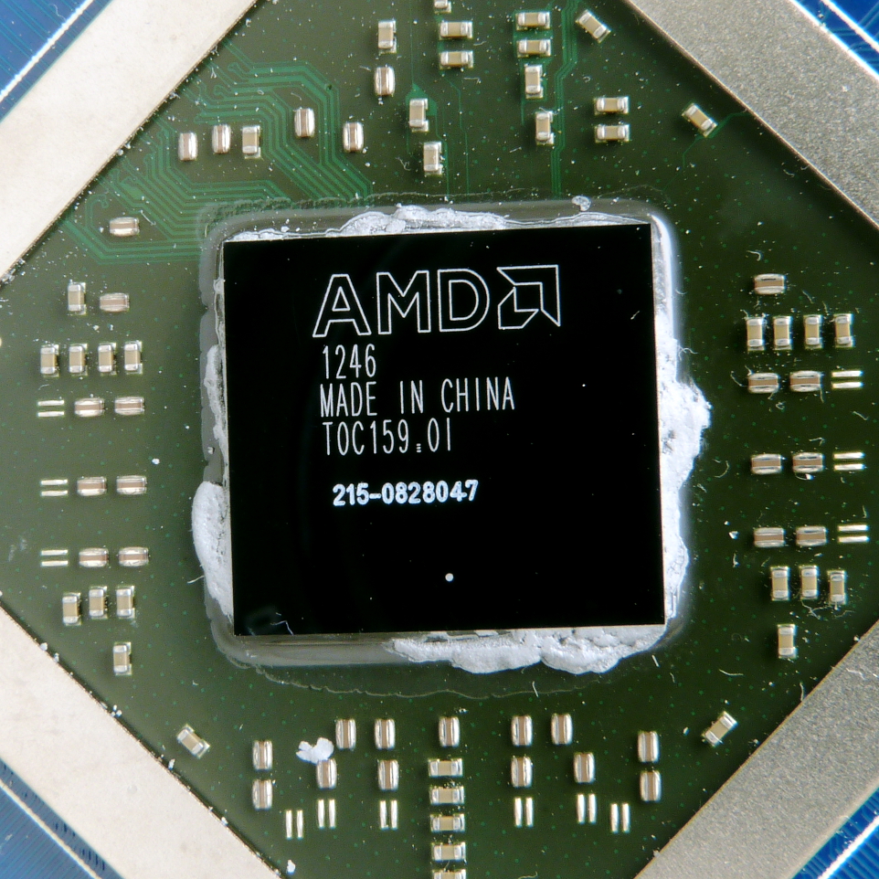 🇺🇸 United StatesRadeon HD 7000 series
AMD graphics processor family using 28 nm process and GCN architectureGPU · GPU architecture · 2012
WorldNVENC
Dedicated video encoding hardware in Nvidia GPUsGPU · GPU architecture · 2012
WorldNvidia Titan
A brand of high-end graphics processing units developed by Nvidia.GPU · 2013