A-RAM
Capacitor-less DRAM cell design using transistor floating bodies
A-RAM is a dynamic random-access memory technology invented in 2009 by researchers in Spain and France. It removes the storage capacitor from standard DRAM cells, using the transistor body itself to hold charge, which helps scaling below 45 nm.
- Invented in 2009 by University of Granada and CNRS
- Uses capacitor-less single-transistor cells for storage
- Targets manufacturing features smaller than 45 nm
- Compatible with SOI, FinFET and MuFET transistors
- A2RAM variant demonstrated in 2012
What it is
A-RAM stands for Advanced-Random Access Memory. It is a specific type of dynamic random-access memory (DRAM) that does not use a separate capacitor to store data. Instead, it relies on single-transistor cells that are capacitor-less. Researchers developed this approach to solve physical limits in memory manufacturing. The technology was created in 2009 through a joint effort between the University of Granada in Spain and the Centre National de la Recherche Scientifique in France. It represents a shift from traditional memory cell designs.
How it came about
The concept emerged in 2009 when engineers identified a bottleneck in shrinking DRAM components. As features moved below 45 nanometres, making tiny capacitors became difficult. Noel Rodriguez and Francisco Gamiz from the University of Granada worked with Sorin Cristoloveanu from CNRS to find a solution. They filed patents for the invention. The team attempted to license the technology to industry partners in 2010. A promotional website managed by the university remained active through that year to share details.
Inside the chip
Standard DRAM uses one transistor and one capacitor per bit. A-RAM removes the capacitor entirely. It stores electrical charge in the floating body of silicon-on-insulator (SOI) transistors. This design fits within the 1T-DRAM family of memories. The structure works with various transistor types, including single-gate SOI, double-gate devices, FinFETs, and multiple-gate field-effect transistors. By using the transistor body for storage, it avoids the miniaturization issues associated with conventional capacitors at small process nodes.
How it was made
The technology targets manufacturing processes with feature sizes under 45 nanometres. It was designed to be compatible with existing advanced transistor architectures like FinFETs. The inventors secured at least one patent for the cell structure. The focus remained on the structural innovation of the memory cell rather than a specific fabrication plant output.
Where it went
This memory type aims to replace high-density dynamic memories in future semiconductor products. It addresses the needs of the industry as devices shrink. The primary application is in systems requiring dense memory storage where traditional capacitors are too large or hard to manufacture. A later version called A2RAM was shown in 2012, suggesting ongoing development for potential integration into chips that need scalable memory solutions without complex capacitor structures.
Versions and family
The original A-RAM design led to a subsequent version known as A2RAM. This variant was demonstrated in 2012. Both belong to the broader 1T-DRAM family, which includes other memories that replace storage capacitors with alternative charge storage methods.
Why it matters
A-RAM offered a potential path for continuing DRAM scaling beyond the 45 nm node. By eliminating the capacitor, it simplified the cell structure for advanced manufacturing. The collaboration between Spanish and French institutions highlighted academic contributions to semiconductor memory design. Although it did not become a dominant industry standard in the provided text, it established a patented approach to capacitor-less memory that influenced later demonstrations like A2RAM.
Questions people ask about A-RAM
What makes A-RAM different from standard DRAM?
Standard DRAM uses a transistor and a capacitor to store each bit of data. A-RAM removes the capacitor entirely. It stores charge in the floating body of the transistor itself, which helps when making components very small.
Who invented A-RAM and where?
It was invented in 2009 by Noel Rodriguez and Francisco Gamiz at the University of Granada in Spain. They collaborated with Sorin Cristoloveanu from the Centre National de la Recherche Scientifique in France.
Why was A-RAM developed?
Researchers saw that making capacitors for DRAM was becoming too difficult as chip features shrank below 45 nanometres. A-RAM solves this miniaturization issue by using the transistor body for storage instead of a separate capacitor.
Good reading and sources
The facts on this page come from the Wikipedia article "A-RAM", written by its contributors and used under the CC BY-SA 4.0 licence, and from its Wikidata record (CC0). EveryChip rewrote the text in its own words, with AI assistance, and compares every page with the article to make sure no passage is copied. It may be reused under the same CC BY-SA 4.0 licence with a link back.
It may contain mistakes, and figures change over time. Nothing here is investment or buying advice. If something is wrong, tell us. Last refreshed 2026-11-14.
Like A-RAM
All memory chips 🇺🇸 United States1T-SRAM
High-density pseudo-static memory technology for embedded systemsMemory · 1998
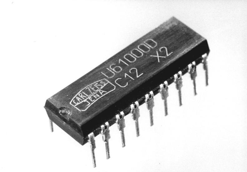 🇩🇪 GermanyU61000
First 1-Mbit DRAM chip from the German Democratic RepublicMemory · 1988